CT3680 Multi-Delay Module V2
Reference and Development Guide
Hardware Rev 2.1C
Firmware Rev 3
July 2026
 |
Overview
The Cabintech CT3680 is a hybrid module that implements from 1 to 4 flexible, configurable audio delay lines. This module can be used by system designers to create many different delay-based effects (reverb, echo, chorus, flanger, etc.) using traditional analog feedback paths, filters, and modulation techniques. Although the CT3680 is digital at its core, all inputs and outputs are analog -- no programming or digital logic design is required and it integrates easily into an analog signal flow. The CT3680 uses a fixed sampling rate that is independent of delay time, producing consistently high quality audio at any delay setting.
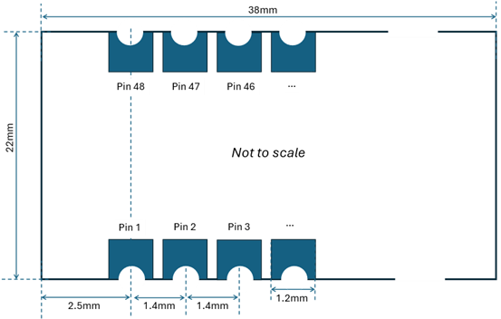
The CT3680 is designed to be easy to use with simple analog audio inputs and outputs, control voltages to set parameter values (such as delay time), and a single +5V power supply. The small module size (22x38mm, 0.9”x1.5”), surface mount edge pins, and through-hole adapter options provide flexibility for mechanical fitment into small spaces and optimize the use of PCB board space.
Audio Inputs/Outputs
The CT3680 has 4 analog audio inputs, and 4 analog audio outputs. The relationship between the inputs and outputs and delay times is controlled by the selected configuration settings. All audio inputs and outputs are line level 2.5V peak, single ended AC coupled (DC offsets removed) for easy integration into an analog signal chain. Traditional analog effects circuits with filtering, modulation, and gain control can be used to create feedback paths for various types of effects.
Configuration
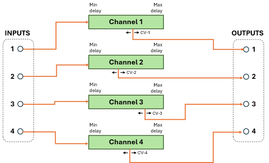
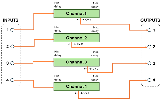
The configuration options control the number of independent delays lines (“channels”) and the maximum delay times they have. Each channel has 1 audio input and 1 or more outputs. Each output has an independent delay control. For example, a channel with 2 outputs would have one input and two outputs assigned to physical AUDIO_OUTPUT_X pins. The outputs are both delays of the same input, but with different delay times, each controlled with a separate CV (control voltage). There are many possible configurations of channels and outputs. For example, one of the configurations is 2 channels with 2 outputs each:
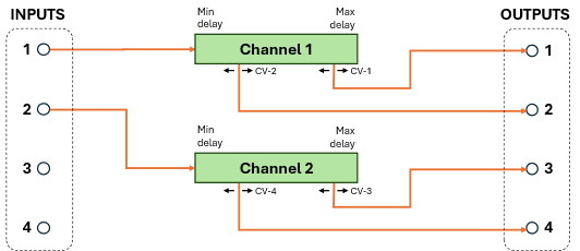
In this configuration, output 1 will be a (variable) delay of input 1. The amount of delay at output 1 is set by a control voltage (CV-1). Output 2 is also a variable delay of input 1, with its own control voltage (CV-2) which sets the delay of output 2. The delays at outputs 1 and 2 are both of the same signal (input 1) but are independently variable. Likewise, outputs 3 and 4 are independent delays of the signal at input 2, controlled by CV-3 and CV-4 respectively. A configuration like this might be used in a true-stereo effect that requires (at least) 2 separate channels of delay.
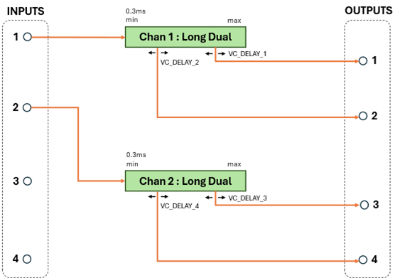
Another configuration consists of 3 independent delay lines, 2 of which have a single delayed output, and 1 has two delayed outputs:
The different configurations can be useful for constructing different types of effects including stereo and effects that utilize multiple delay lines.
Configuration is done with 4 input pins that choose between different “programs”, each of which defines a specific configuration. In addition, 5 “option” input pins control additional features depending on the selected program. See Program Selection on page 15 for a description of all the available programs.
Additional inputs select the audio sampling rate (48kHz, 32kHz, 24kHz, 12kHz). Lower sampling rates allow for longer delay times. The sampling rate remains fixed at the selected rate (e.g. sampling rate is not used to vary the delay time as in traditional BBD devices). See Sampling Rate Selection on page 14.
Delay Control
The selection of configuration and sampling rate defines the minimum and maximum delay of each channel in the configuration. The outputs for that channel can have any delay time between the min and max, and the delay time can vary dynamically by use of control voltages (CVs).
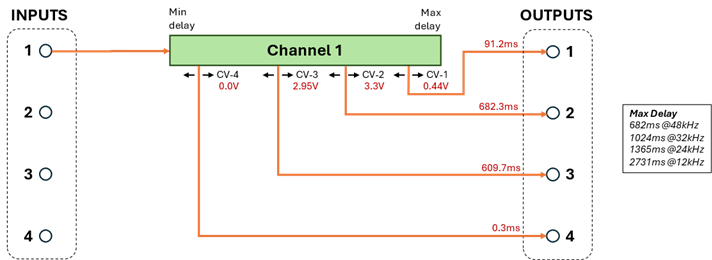
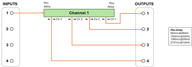
A delay CV is an input voltage in the range of 0.0V to 3.3V. When the CV is at 0.0V then the corresponding output is at the minimum delay. When the CV is at the maximum of 3.3V then the output is at the maximum delay. Voltage levels between 0.0 and 3.3 form a linear scaling of delay time between min and max. (Preview feature: An exponential scaling can also be enabled, see Setting Delay Times on page 47). For example, the following channel configuration has 1 input and 4 outputs controlled by CV-1 through CV-4. With a sampling rate of 48kHz this channel has a max delay of 682ms and a min delay of 0.3ms.
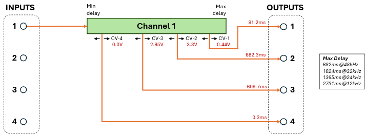
With the control voltage values shown, the outputs have the delays shown0F[1]. Note that the line positions as drawn in the diagram are conceptual and not drawn in proportion to the actual delay time. E.g. the line for output 1 is drawn to the right of channel 2 on the green channel bar (closer to Max delay), but actually has a shorter delay time. The CV for any output can select any delay time in the range from min to max, independent of all other outputs.
Also see Setting Delay Times on page 47.
Additional Features
Some programs (configurations) support additional features. These features are optional and enabled using the 5 OPTION input pins. See the individual program descriptions to see what features are supported in which programs.
·
Tap tempo: Some programs support setting delay time based
on a tapped input (e.g. pressing (tapping) a momentary button). The tap
interval can be used to scale CV-controlled delay times, or create delays at
fixed musical intervals (e.g. quarter note delays, dotted-eighth note delays,
etc). See Tap Tempo Feature on page 43.
·
Simulated aliasing: Some programs support the ability to
simulate sampling-rate aliasing similar to the aliasing distortion that occurs
in BBD devices when run at lower clock (sampling) rates. In some effects this
distortion is desirable and is part of the overall sonic design. The amount of
aliasing distortion can be manually controlled by CV or automatically
determined by the delay settings. Aliasing distortion is disabled by default.
See Aliasing Feature on page 45. And the Pinout link as well.
·
Mono-to-stereo effects: Some programs perform mono-input
to stereo-output conversion using a Haas delay effect. The left-right spread of
the stereo effect can be varied and is controlled by a CV input.
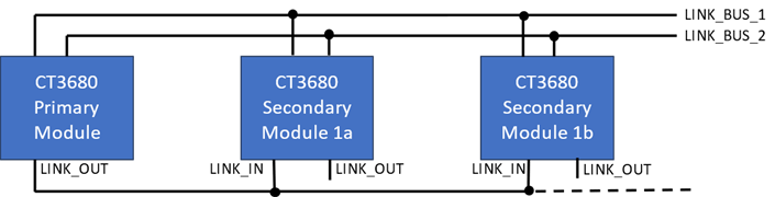
· Chaining: Multiple CT3680 modules can be “chained” together to achieve very long delay times and more inputs and outputs. Audio signals are passed digitally through the chain so there is no loss in fidelity no matter how many modules are linked together. See Chaining Multiple Modules on page 49.
Design Requirements
The CT3680 is designed to minimize external component requirements and integrate easily into effects designs. The CT3680 requires no external clock and is powered by +5V. All CV signals are +3.3V maximum (see Specifications and Maximum Ratings on page 13). A +3.3V reference is made available on an output pin to aid in generating CV signals. All audio analog inputs and outputs are single-ended, 2.5V full scale, and AC coupled. Clipping is detected and signaled on an output pin and an onboard LED. All digital configuration input pins have pull-up or pull-down resistors such that leaving them unconnected produces a good default configuration.
The physical package is a 48 pin surface mount castellated-edge pin module. It can easily be hand soldered or soldered in automated systems. A 48-pin standard DIL spacing through-hole adapter is available for through-hole PCB designs or breadboard prototyping. A full development/breakout board is available with switches and potentiometers to control all module inputs, header pins for probe points, and 3.5mm input and output jacks for easy connection to other equipment.
Features
· 4 analog audio inputs and 4 analog audio outputs
· 6 control voltage (CV) inputs to set delay time and other parameters
· >92dB signal-to-noise ratio (SNR) with less than 0.0009% THD
· Frequency response +/-0.5dB, 20-20kHz
· Selectable configurations for 1, 2, 3, or 4 independent delay lines
· Maximum delay of 2.7 seconds (divided between all delay lines)
· Tap tempo input and tap-flash LED output
· Optional simulated aliasing distortion
· Optional mono-to-stereo conversion on some programs
· Selectable sampling rates of 48kHz (default), 32kHz, 24kHz, or 12kHz
· Digitally chainable up to 5 modules with total max delay of 13.5 seconds
· No external clock is required
· +5V power (~170mA)
· Reverse voltage protection
· Clipping-detected output signal and on-board clipping LED
· Emulation of any BBD model MN3001 to MN3011 plus SAD512, SAD1024, TDA1022, V3205, V3207, V3208
· Castellated edges for direct soldering to a PCB (through-hole adapter is available)
· Updatable firmware
Pinout
|
|
||||||
|
|
|
|
|
|
||
|
AUDIO_IN_1 ► |
1 |
48 |
|
|||
|
AUDIO_IN_2 ► |
2 |
47 |
|
|||
|
AUDIO_OUT_1 ◄ |
3 |
46 |
|
|||
|
AUDIO_OUT_2 ◄ |
4 |
45 |
|
|||
|
N.C. |
5 |
44 |
N.C. |
|||
|
N.C. |
6 |
43 |
N.C. |
|||
|
LINK_1CH ► |
7 |
42 |
N.C. |
|||
|
+5V ► |
8 |
41 |
|
|||
|
+5V ► |
9 |
40 |
|
|||
|
I2C_SCL ► |
10 |
39 |
|
|||
|
I2C_SDA ◄► |
11 |
38 |
|
|||
|
PGM0 ► |
12 |
37 |
|
|||
|
PGM1 ► |
13 |
36 |
|
|||
|
PGM2 ► |
14 |
35 |
|
|||
|
PGM3 ► |
15 |
34 |
|
|||
|
REF_3V3 ◄ |
16 |
33 |
|
|||
|
VC_DELAY_4 ► |
17 |
32 |
|
|||
|
VC_DELAY_3 ► |
18 |
31 |
|
|||
|
VC_DELAY_2 ► |
19 |
30 |
|
|||
|
VC_DELAY_1 ► |
20 |
29 |
|
|||
|
VC_SCALE_MAX ► |
21 |
28 |
N.C. |
|||
|
VC_SCALE_MIN ► |
22 |
27 |
|
|||
|
GND ► |
23 |
26 |
|
|||
|
GND ► |
24 |
25 |
|
|||
|
|
|
|
|
|||
|
◄ ► Input, Output
|
||||||
Pin Descriptions
|
Pin |
I/O |
Symbol |
Description |
|||||||||||||||
|
1 |
In |
AUDIO_IN_1 |
Audio input 1 |
|||||||||||||||
|
2 |
In |
AUDIO_IN_2 |
Audio input 2 |
|||||||||||||||
|
3 |
Out |
AUDIO_OUT_1 |
Audio output 1 |
|||||||||||||||
|
4 |
Out |
AUDIO_OUT_2 |
Audio output 2 |
|||||||||||||||
|
5 |
- |
N.C. |
Leave unconnected |
|||||||||||||||
|
6 |
- |
N.C. |
Leave unconnected |
|||||||||||||||
|
7 |
In |
LINK_1CH |
Number of
channels linked in a secondary module (internal
pullup) |
|||||||||||||||
|
8 |
- |
5V |
+5V supply |
|||||||||||||||
|
9 |
- |
5V |
+5V supply |
|||||||||||||||
|
10 |
- |
I2C_SCL |
It is recommended to bring these pins (and GND) to a 3-pin header to install future firmware updates. See Firmware Updates on page 56. |
|||||||||||||||
|
11 |
- |
I2C_SDA |
||||||||||||||||
|
12 |
In |
PGM0 |
Bit 0 (lsb) of program number (internal pulldown) |
|||||||||||||||
|
13 |
In |
PGM1 |
Bit 1 of program number (internal pulldown) |
|||||||||||||||
|
14 |
In |
PGM2 |
Bit 2 of program number (internal pulldown) |
|||||||||||||||
|
15 |
In |
PGM3 |
Bit 3 (msb) of program number (internal pulldown) |
|||||||||||||||
|
16 |
Out |
REF_3V3 |
+3.3V output reference (40mA max) |
|||||||||||||||
|
17 |
In |
VC_DELAY_4 |
Set delay time within the global time scale |
|||||||||||||||
|
18 |
In |
VC_DELAY_3 |
Set delay time within the global time scale |
|||||||||||||||
|
19 |
In |
VC_DELAY_2 |
Set delay time within the global time scale |
|||||||||||||||
|
20 |
In |
VC_DELAY_1 |
Set delay time within the global time scale |
|||||||||||||||
|
21 |
In |
VC_SCALE_MAX |
Global scalar for maximum delay time |
|||||||||||||||
|
22 |
In |
VC_SCALE_MIN |
Global scalar for minimum delay time |
|||||||||||||||
|
23 |
- |
GND |
Ground |
|||||||||||||||
|
24 |
- |
GND |
Ground |
|||||||||||||||
|
25 |
In |
RESET |
Pull low for 1ms or longer to reset (internal pullup) |
|||||||||||||||
|
26 |
In |
RATE_1 |
Set audio sampling rate, takes effect on next reset or power on (internal pullup)
|
|||||||||||||||
|
27 |
In |
RATE_0 |
||||||||||||||||
|
28 |
- |
N.C. |
Leave unconnected |
|||||||||||||||
|
29 |
Out |
CLIPPING |
Hardware rev 1.0: Low current1 CLIPPING LED output Hardware rev 2.1C: Clipping LED output can sink 0.8mA max |
|||||||||||||||
|
30 |
In |
OPTION_5 |
Digital control inputs (usage depends on the selected program). These inputs have internal pullups and register as HIGH when disconnected. |
|||||||||||||||
|
31 |
In |
OPTION_4 |
||||||||||||||||
|
32 |
In |
OPTION_3 |
||||||||||||||||
|
33 |
In |
OPTION_2 |
||||||||||||||||
|
34 |
In |
OPTION_1 |
||||||||||||||||
|
35 |
In |
TT |
Tap tempo (internal pullup) |
|||||||||||||||
|
36 |
In |
PRIMARY |
Sets this module mode to PRIMARY (high) or SECONDARY (low). See Chaining Multiple Modules on page 49. Changes take effect on next RESET or power on. (internal pullup) |
|||||||||||||||
|
37 |
Out |
LINK_OUT |
N.C. on single modules or the last module in a multi-module configuration. Connected to downstream module’s LINK_IN in multi-module configurations. |
|||||||||||||||
|
38 |
In |
LINK_IN |
N.C. on single modules or the primary module in a multi-module configuration. Connected to the upstream module’s LINK_OUT in multi-module configurations. |
|||||||||||||||
|
39 |
In/Out |
LINK_BUS_2 |
N.C. on single modules. Connected to all module’s LINK_BUS2 pins in multi-module configurations. |
|||||||||||||||
|
40 |
In/Out |
LINK_BUS_1 |
N.C. on single modules. Connected to all module’s LINK_BUS1 pins in multi-module configurations. |
|||||||||||||||
|
41 |
- |
TT_FLASH |
Hardware rev 1.0: N.C. Hardware rev 2.1: Low current1 tap-temp flasher LED output Hardware rev 2.1C: Tap-tempo flasher LED output, 0.8mA max sink. |
|||||||||||||||
|
42 |
- |
N.C. |
Leave unconnected |
|||||||||||||||
|
43 |
- |
N.C. |
Leave unconnected |
|||||||||||||||
|
44 |
- |
N.C. |
Leave unconnected |
|||||||||||||||
|
45 |
Out |
AUDIO_OUT_4 |
Audio output 4 |
|||||||||||||||
|
46 |
Out |
AUDIO_OUT_3 |
Audio output 3 |
|||||||||||||||
|
47 |
In |
AUDIO_IN_3 |
Audio input 3 |
|||||||||||||||
|
48 |
In |
AUDIO_IN_4 |
Audio input 4 |
Notes:
1Hardware rev 2.1 --
Pins 29 and 41 are low-current outputs not suitable for direct driving a
typical LED. See the PCB Design Notes on page 55 for driver circuit example. Starting with rev 2.1C these outputs can directly
drive an LED at 0.8mA sink max and no external driver circuit is required.
N.C. pins must be left
unconnected.
Unused audio and CV inputs
should be tied to ground to minimize noise.
Unused outputs should be left unconnected.
Specifications and Maximum Ratings
|
Item |
Symbol |
Range |
Notes |
|
Supply voltage |
5V |
+4.5 to +5.5V |
|
|
Supply current |
|
160-180mA |
|
|
CV input voltage range |
VC_* |
0 to REF_3V3 |
See Note 3 |
|
Audio input |
AUDIO_IN_* |
0 to 2.6V p-p |
AC coupled, see Note 1 |
|
Audio output |
AUDIO_OUT_* |
-1.25V to +1.25V (2.5V p-p ) |
AC coupled, see Note 2 |
|
Audio input impedance |
|
7-10kΩ |
|
|
Audio output load impedance |
|
5kΩ |
Min |
|
Signal to Noise Ratio 1 |
|
> 92dB |
|
|
Noise floor |
|
< -104dB |
|
|
THD 1 |
|
< 0.0009% |
|
|
Frequency response |
|
20Hz - 20kHz |
+/- 0.5dB |
All measurements are unweighted, 48kHz sampling rate
1 At 1kHz
Notes
1.
Audio inputs are AC coupled; any DC offset (bias) component of
the input signal is removed and does not affect operation of the CT3680. The
remaining (AC) portion of the signal must not exceed the maximum input
specification of 2.6V peak to peak.
2.
Audio outputs are AC coupled and will contain no DC offset. The
AC output signal will be centered around 0V (ground) with a maximum amplitude
of -1.25V to +1.25V (for a total of 2.5V peak to peak). If subsequent circuits
require positive-only signals the CT3680 audio outputs will need to be biased
at least +1.25V to keep them above 0V.
3. Input control voltages (e.g. CV_* pins) should be referenced to the CT3680 REF_3V3 pin (e.g. they should not exceed the voltage at REF_3V3).
Sampling Rate Selection
The CT3680 (hardware version 2.0A and later) supports four sampling rates, selected by the RATE_0 and RATE_1 input pins. Changes to the sampling rate take effect at the next RESET or power on (sample rate does not change dynamically). The choice of sampling rate defines the range of possible delays that can be achieved and the quality of the audio.
Choosing a sampling rate defines the minimum and maximum total available delay. The actual delay at any particular output depends on the CV inputs and determined by the currently running program (see Program Selection on page 15). Unlike BBD devices, sampling rate is not used to dynamically alter (modulate) the delay time. The sampling rate stays fixed until the module is RESET or power cycled. Delay modulation is achieved by changes in the CV inputs.
By selecting a lower sampling rate, less memory is required to store (delay) samples per second, so longer delays can be achieved. This is a tradeoff between longer delay times and higher fidelity – audio quality decreases with lower sampling rates.
The following table shows the sampling rates and min/max delays that are selected by the RATE_1 and RATE_0 pins.
|
Sampling |
Min |
Total Max |
||
|
1 |
0 |
|||
|
0 |
0 |
12kHz |
1.16ms |
2.731s |
|
0 |
1 |
24kHz |
0.58ms |
1.365s |
|
1 |
0 |
32kHz |
0.44ms |
1.024s |
|
1 |
1 |
48kHz |
0.29ms |
0.682s |
“Total Max Delay” is the total delay time of all channels combined. How this total delay time is divided among the delay channels is defined by the selected program. For example, program 0 allocates all the available delay time to a single channel with 4 outputs. Program 3 divides all the delay time equally among 4 independent channels (so for example, if the sample rate is 24kHz, that program will allocate 1.37s / 4 = 344ms to each channel). See the program descriptions to see how the total available delay time is allocated for each program.
When multiple modules are chained together (see Chaining Multiple Modules on page 49) all modules will operate at the same sampling rate as set on the PRIMARY module.
The RATE_0 and RATE_1 pins have an internal pull-up resistor, so if left unconnected the module will operate at the 48kHz sampling rate.
Program Selection
Configuration of the module is done by selecting 1 of 16 “programs” using the 4 PGM input pins. The selected program defines the basic topology of the delay lines (number of channels, number of outputs per channel, etc.) and the optional features that are available. The selected program can be changed at any time. When the program is changed, the current delay buffer is cleared, the new program is loaded, and input samples begin to be processed into the delay buffer. The PGM pins have an internal pull-down resistor, so if left unconnected program 0 will be selected.
Summary of Programs
The following table is a quick summary of the available programs. The first 4 programs (0-3) provide basic delays in various combinations of channels and outputs/channel. Additional programs (4+) are more advanced and provide specialized features and effects. The sections that follow describe each program in more detail including how they define the channels, delay times, and various options.
|
Basic Programs |
Program 0 1 Channel |
Program 1 2 Channels |
Program 2 3 Channels |
Program 3 4 Channels |
|
|
Channels (inputs) |
1 |
2 |
3 |
4 |
|
|
Outputs per Channel |
4 |
2 |
1 (2 on ch 3) |
1 |
|
|
Max Delay per |
48kHz |
682ms |
341ms |
227ms |
170ms |
|
32kHz |
1025ms |
512ms |
341ms |
256ms |
|
|
24kHz |
1365ms |
682ms |
455ms |
341ms |
|
|
12kHz |
2731ms |
1366ms |
910ms |
383ms |
|
|
Optional Features |
Global scalars |
|
|
|
|
|
Tap tempo |
|
|
|
|
|
|
Manual Aliasing |
|
|
|
|
|
|
Auto Aliasing |
|
|
|
|
|
|
Mono to stereo |
|
|
|
|
|
|
Exponential CV |
|
|
|
|
|
|
Advanced Programs |
Program 4 2 Channels + Stereo |
Program 5 MN3011 Emulation |
Program 6 BBD Emulation |
Program
7 |
Program 8 Multi-Effects 2 |
|
|
Channels (inputs) |
3 |
1 |
4 |
Varies by option |
Varies by option |
|
|
Outputs per Channel |
1 |
4/6 * |
1 |
|||
|
Max Delay per |
48kHz |
326ms |
682ms |
Varies by option |
||
|
32kHz |
489ms |
- |
||||
|
24kHz |
653ms |
- |
||||
|
12kHz |
1205ms |
- |
||||
|
Optional Features |
Global scalars |
|
|
|
|
|
|
Tap tempo |
|
|
|
|
|
|
|
Manual Aliasing |
|
|
|
|
|
|
|
Auto Aliasing |
|
|
|
|
|
|
|
Mono to stereo |
|
|
|
|
|
|
|
Exponential CV |
|
|
|
|
|
|
* 4 outputs with 1 module or 6 outputs with 2 modules
Program 0 : One Delay Line
This program provides a single delay line with a maximum delay time of 100% of the total available. Audio inputs 2, 3, and 4 are unused. This program supports the Tap Tempo Feature (page 43) and Aliasing Feature (page 44).
|
Sample |
Max Delay |
|
48kHz |
682ms |
|
32kHz |
1.024s |
|
24kHz |
1.365s |
|
12kHz |
2.731s |
|
Program 0 Pin Usage |
||||||||||||||||||||||||||||||
|
Pin # |
Pin Type and Name |
Function |
Notes |
|||||||||||||||||||||||||||
|
1 |
|
Chan 1 Input |
|
|||||||||||||||||||||||||||
|
2 |
|
Unused |
|
|||||||||||||||||||||||||||
|
46 |
|
Unused |
|
|||||||||||||||||||||||||||
|
45 |
|
Unused |
|
|||||||||||||||||||||||||||
|
3 |
|
Chan 1 Output 1 |
|
|||||||||||||||||||||||||||
|
4 |
|
Chan 1 Output 2 |
|
|||||||||||||||||||||||||||
|
46 |
|
Chan 1 Output 3 |
|
|||||||||||||||||||||||||||
|
45 |
|
Chan 1 Output 4 |
|
|||||||||||||||||||||||||||
|
20 |
|
Delay 1 Control |
|
|||||||||||||||||||||||||||
|
19 |
|
Delay 2 Control |
|
|||||||||||||||||||||||||||
|
18 |
|
Delay 3 Control |
|
|||||||||||||||||||||||||||
|
17 |
|
Delay 4 Control |
Alias intensity control when OPTION_5=0 |
|||||||||||||||||||||||||||
|
22 |
|
Global Delay Min |
|
|||||||||||||||||||||||||||
|
21 |
|
Global Delay Max |
|
|||||||||||||||||||||||||||
|
34 |
|
Bit 0 |
Selects 1 of 8 tap tempo dividers
|
|||||||||||||||||||||||||||
|
33 |
|
Bit 1 |
||||||||||||||||||||||||||||
|
32 |
|
Bit 2 |
||||||||||||||||||||||||||||
|
31 |
|
Exponential Delay CVs |
PREVIEW FEATURE 1=Disabled, 0=Enabled |
|||||||||||||||||||||||||||
|
30 |
|
Aliasing |
1=Disabled, 0=Enabled |
|||||||||||||||||||||||||||
|
35 |
|
Tap tempo switch input |
|
|||||||||||||||||||||||||||
|
41 |
|
Tap tempo LED output |
|
|||||||||||||||||||||||||||
AUDIO_IN_1 is the delay line input, all other audio inputs are unused. Four independently controlled delay outputs are available (all outputs are a delayed copy of input 1). In normal operation mode (tap-tempo not engaged), each output is an independent delay of input #1 controlled by the corresponding VC_DELAY_# voltage. A control voltage of zero produces the minimum delay, and a control voltage of REF_3V3 (3.3V) produces the maximum delay on that output. For example, at 32kHz sample rate (1.024ms max delay), setting VC_DELAY_2 to 1.0V would produce a delay on output 2 of (1.0V/3.3V) x 1.024s = 0.31s. For a complete description of how delays are calculated, including effect of global scalars, see Setting Delay Times on page 47.
Note there is no required ordering of delayed outputs, e.g. delay 1 could be longer than delay 3. All the outputs are independently controlled by their corresponding CV delay voltage and changing one CV value does not affect the delay at the other outputs.
When tap-temp is engaged the global MIN/MAX CV inputs are ignored; MIN is set to zero, and the global MAX delay time is set to the tap interval divided by 1 of 8 possible musical intervals. The divider value is selected by OPTION pins 1, 2, and 3. The result of that division becomes the global MAX delay time (the global MIN delay time is set to zero). Note that the delay CV inputs 1-4 continue to define the delays of the 4 outputs. Just like the non-tap mode they are scaled to the range of global MIN (zero) to global MAX (tap interval / divider). Thus the tap interval affects the delay for all 4 outputs. See the Tap Tempo Feature on page 43 and the Tap to Max method for more details.
When the aliasing feature is enabled by holding the OPTION_5 pin low:
· all outputs will have an equal controlled amount of aliasing effect applied, and
· VC_DELAY_4 will control the intensity of the aliasing effect (this is referred to as Manual Aliasing Mode), and
· VC_SCALE_MAX will control the amount of delay on output 4 (since VC_DELAY_4 is used for aliasing). E.g. output 4 will track the global maximum delay.
See the Aliasing Feature description on page 45 for more details.
PREVIEW FEATURE When the exponential scaling feature is enabled by holding the OPTION_4 pin low, the CV_DELAY_X inputs will have exponential delay-time scaling. See Setting Delay Times on page 47. This feature does not affect the VC_SCALE_MIN or VC_SCALE_MAX inputs.
Program 1 :Two Delay Lines
This program is 2 independent delay channels with 2 outputs each. Each channel has a maximum delay time of 50% of the total available. This program supports the Tap Tempo Feature (page 43) and Aliasing Feature (page 44).
|
Sample |
Max Delay |
|
48kHz |
341ms |
|
32kHz |
512ms |
|
24kHz |
683ms |
|
12kHz |
1.366s |
|
Program 1 Pin Usage |
||||||||||||||||||||||||||||||
|
Pin # |
Pin Name |
Function |
Notes |
|||||||||||||||||||||||||||
|
1 |
|
Chan 1 Input |
|
|||||||||||||||||||||||||||
|
2 |
|
Chan 2 Input |
|
|||||||||||||||||||||||||||
|
46 |
|
Unused |
|
|||||||||||||||||||||||||||
|
45 |
|
Unused |
|
|||||||||||||||||||||||||||
|
3 |
|
Chan 1 Delay 1 Output |
|
|||||||||||||||||||||||||||
|
4 |
|
Chan 1 Delay 2 Output |
|
|||||||||||||||||||||||||||
|
46 |
|
Chan 2 Delay 1 Output |
|
|||||||||||||||||||||||||||
|
45 |
|
Chan 2 Delay 2 Output |
|
|||||||||||||||||||||||||||
|
20 |
|
Chan 1 Delay 1 Control |
|
|||||||||||||||||||||||||||
|
19 |
|
Chan 1 Delay 2 Control |
|
|||||||||||||||||||||||||||
|
18 |
|
Chan 2 Delay 1 Control |
|
|||||||||||||||||||||||||||
|
17 |
|
Chan 2 Delay 2 Control |
Alias intensity control when OPTION_5=0 |
|||||||||||||||||||||||||||
|
22 |
|
Global Delay Min |
|
|||||||||||||||||||||||||||
|
21 |
|
Global Delay Max |
|
|||||||||||||||||||||||||||
|
34 |
|
Bit 0 |
Selects 1 of 8 tap tempo dividers
|
|||||||||||||||||||||||||||
|
33 |
|
Bit 1 |
||||||||||||||||||||||||||||
|
32 |
|
Bit 2 |
||||||||||||||||||||||||||||
|
31 |
|
Exponential Delay CVs |
PREVIEW FEATURE 1=Disabled, 0=Enabled |
|||||||||||||||||||||||||||
|
30 |
|
Aliasing |
1=Disabled, 0=Enabled |
|||||||||||||||||||||||||||
|
35 |
|
Tap tempo switch input |
|
|||||||||||||||||||||||||||
|
41 |
|
Tap tempo LED output |
|
|||||||||||||||||||||||||||
AUDIO_INPUT_1 and AUDIO_INPUT_2 are the inputs to the 2 channels, all other audio inputs are unused. Channel 1 has two outputs provided at AUDIO_OUT_1 and AUDIO_OUT_2. Channel 2’s outputs are AUDIO_OUT_3 and AUDIO_OUT_4. All delays for all channels are bounded by the global MIN/MAX scalars.
When tap-temp is engaged the global MIN/MAX CV inputs are ignored; MIN is set to zero and the global MAX delay time is set to the tap interval divided by 1 of 8 possible musical intervals. The divider value is selected by OPTION pins 1, 2, and 3. The result of that division becomes the global MAX delay time (MIN delay time is set to zero). Note that the delay CV inputs 1-4 continue to define the delays of the 4 outputs. Just like the non-tap mode they are scaled to the range of global MIN (zero) to global MAX (tap interval / divider). Thus the tap interval affects the delay for all 4 outputs. See the Tap Tempo Feature on page 43 and the Tap to Max method for more details.
When the aliasing feature is enabled by holding the OPTION_5 pin low:
· all outputs will have an equal controlled amount of aliasing effect applied, and
· VC_DELAY_4 will control the intensity of the aliasing effect (this is referred to as Manual Aliasing Mode), and
· VC_SCALE_MAX will control the amount of delay on output 4 (since VC_DELAY_4 is used for aliasing). E.g. output 4 will track the global maximum delay.
See the Aliasing Feature description on page 45 for more details.
PREVIEW FEATURE When the exponential scaling feature is enabled by holding the OPTION_4 pin low, the CV_DELAY_X inputs will have exponential delay-time scaling. See Setting Delay Times on page 47. This feature does not affect the VC_SCALE_MIN or VC_SCALE_MAX inputs.
Program 2 : Three Delay Lines
|
Sample |
Max Delay |
|
48kHz |
227ms |
|
32kHz |
341ms |
|
24kHz |
455ms |
|
12kHz |
910ms |
This program is 3 independent delay channels with 1 output on channels 1 and 2,
and 2 outputs on channel 3. Each channel has a maximum delay time of 33% of the
total available. This program supports the Tap
Tempo Feature (page 43) and Aliasing Feature (page 44).
|
Program 2 Pin Usage |
||||||||||||||||||||||||||||||
|
Pin # |
Pin Name |
Function |
Notes |
|||||||||||||||||||||||||||
|
1 |
|
Chan 1 Input |
|
|||||||||||||||||||||||||||
|
2 |
|
Chan 2 Input |
|
|||||||||||||||||||||||||||
|
46 |
|
Chan 3 Input |
|
|||||||||||||||||||||||||||
|
45 |
|
Unused |
|
|||||||||||||||||||||||||||
|
3 |
|
Chan 1 Output |
|
|||||||||||||||||||||||||||
|
4 |
|
Chan 2 Output |
|
|||||||||||||||||||||||||||
|
46 |
|
Chan 3 Output 1 |
|
|||||||||||||||||||||||||||
|
45 |
|
Chan 3 Output 2 |
|
|||||||||||||||||||||||||||
|
20 |
|
Chan 1 Delay Control |
|
|||||||||||||||||||||||||||
|
19 |
|
Chan 2 Delay Control |
|
|||||||||||||||||||||||||||
|
18 |
|
Chan 3 Delay 1 Control |
|
|||||||||||||||||||||||||||
|
17 |
|
Chan 3 Delay 2 Control |
Alias intensity control when OPTION_5=0 |
|||||||||||||||||||||||||||
|
22 |
|
Global Delay Min |
|
|||||||||||||||||||||||||||
|
21 |
|
Global Delay Max |
|
|||||||||||||||||||||||||||
|
34 |
|
Bit 0 |
Selects 1 of 8 tap tempo dividers
|
|||||||||||||||||||||||||||
|
33 |
|
Bit 1 |
||||||||||||||||||||||||||||
|
32 |
|
Bit 2 |
||||||||||||||||||||||||||||
|
31 |
|
Exponential Delay CVs |
PREVIEW FEATURE 1=Disabled, 0=Enabled |
|||||||||||||||||||||||||||
|
30 |
|
Aliasing |
1=Disabled, 0=Enabled |
|||||||||||||||||||||||||||
|
35 |
|
Tap tempo switch input |
|
|||||||||||||||||||||||||||
|
41 |
|
Tap tempo LED output |
|
|||||||||||||||||||||||||||
This program provides 3 independent delay channels. The first 2 channels (AUDIO_INPUT_1/2) have a single delayed output each (AUDIO_OUT_1/2). The third channel has 2 delayed outputs (ADUIO_OUT_3/4) controlled by VC_DELAY_3 and VC_DELAY_4. The maximum delay time for each channel is 1/3 of the total available. The global MIN/MAX scalars apply to all delay times.
When tap-temp is engaged the global MIN/MAX CV inputs are ignored and the global MAX delay time is set to the tap interval divided by 1 of 8 possible musical intervals. The divider value is selected by OPTION pins 1, 2, and 3. The result of that division becomes the global MAX delay time, and the global MIN delay time is set to zero. Note that the delay CV inputs 1-4 continue to define the delays of the 4 outputs. Just like the non-tap mode they are scaled to the range of global MIN (zero) to global MAX (tap interval / divider). Thus the tap interval affects the delay for all 4 outputs. See the Tap Tempo Feature on page 43 and the Tap to Max method for more details.
When the aliasing feature is enabled by holding the OPTION_5 pin low:
· all outputs will have an equal controlled amount of aliasing effect applied, and
· VC_DELAY_4 will control the intensity of the aliasing effect (this is referred to as Manual Aliasing Mode), and
· VC_SCALE_MAX will control the amount of delay on output 4 (since VC_DELAY_4 is used for aliasing). E.g. output 4 will track the global maximum delay.
See the Aliasing Feature description on page 45 for more details.
PREVIEW FEATURE When the exponential scaling feature is enabled by holding the OPTION_4 pin low, the CV_DELAY_X inputs will have exponential delay-time scaling. See Setting Delay Times on page 47. This feature does not affect the VC_SCALE_MIN or VC_SCALE_MAX inputs.
Program 3 : Four Delay Lines
This program provides 4 independent delay channels each with a maximum delay time of 25% of the total available. This program supports the Tap Tempo Feature (page 43) and the Aliasing Feature (page 45).
|
Sample |
Max Delay |
|
48kHz |
170ms |
|
32kHz |
256ms |
|
24kHz |
341ms |
|
12kHz |
383ms |
|
Program 3 Pin Usage |
||||||||||||||||||||||||||||||
|
Pin # |
Pin Name |
Function |
Notes |
|||||||||||||||||||||||||||
|
1 |
|
Audio Input 1 |
|
|||||||||||||||||||||||||||
|
2 |
|
Audio Input 2 |
|
|||||||||||||||||||||||||||
|
46 |
|
Audio Input 3 |
|
|||||||||||||||||||||||||||
|
45 |
|
Audio Input 4 |
|
|||||||||||||||||||||||||||
|
3 |
|
Chan 1 Output |
|
|||||||||||||||||||||||||||
|
4 |
|
Chan 2 Output |
|
|||||||||||||||||||||||||||
|
46 |
|
Chan 3 Output |
|
|||||||||||||||||||||||||||
|
45 |
|
Chan 4 Output |
|
|||||||||||||||||||||||||||
|
20 |
|
Chan 1 Delay Control |
|
|||||||||||||||||||||||||||
|
19 |
|
Chan 2 Delay Control |
|
|||||||||||||||||||||||||||
|
18 |
|
Chan 3 Delay Control |
|
|||||||||||||||||||||||||||
|
17 |
|
Chan 4 Delay Control |
Alias intensity control when OPTION_5=0 |
|||||||||||||||||||||||||||
|
22 |
|
Global Delay Min |
|
|||||||||||||||||||||||||||
|
21 |
|
Global Delay Max |
|
|||||||||||||||||||||||||||
|
34 |
|
Bit 0 |
Selects 1 of 8 tap tempo dividers
|
|||||||||||||||||||||||||||
|
33 |
|
Bit 1 |
||||||||||||||||||||||||||||
|
32 |
|
Bit 2 |
||||||||||||||||||||||||||||
|
31 |
|
Exponential Delay CVs |
PREVIEW FEATURE 1=Disabled, 0=Enabled |
|||||||||||||||||||||||||||
|
30 |
|
Aliasing |
1=Disabled, 0=Enabled |
|||||||||||||||||||||||||||
|
35 |
|
Tap tempo switch input |
|
|||||||||||||||||||||||||||
|
41 |
|
Tap tempo LED output |
|
|||||||||||||||||||||||||||
Each channel has a single delayed output controlled by the corresponding VC_DELAY_x value. The global MIN/MAX scalars apply to all delay times.
When tap-temp is engaged the global MIN/MAX CV inputs are ignored and the global MAX delay time is set to the tap interval divided by 1 of 8 possible musical intervals. The divider value is selected by OPTION pins 1, 2, and 3. The result of that division becomes the global MAX delay time, and the global MIN delay time is set to zero. Note that the delay CV inputs 1-4 continue to define the delays of the 4 outputs. Just like the non-tap mode they are scaled to the range of global MIN (zero) to global MAX (tap interval / divider). Thus the tap interval affects the delay for all 4 outputs. See the Tap Tempo Feature on page 43 and the Tap to Max method for more details.
When the aliasing feature is enabled by holding the OPTION_5 pin low:
· all outputs will have an equal controlled amount of aliasing effect applied, and
· VC_DELAY_4 will control the intensity of the aliasing effect (this is referred to as Manual Aliasing Mode), and
· VC_SCALE_MAX will control the amount of delay on output 4 (since VC_DELAY_4 is used for aliasing). E.g. output 4 will track the global maximum delay.
See the Aliasing Feature description on page 45 for more details.
PREVIEW FEATURE When the exponential scaling feature is enabled by holding the OPTION_4 pin low, the CV_DELAY_X inputs will have exponential delay-time scaling. See Setting Delay Times on page 47. This feature does not affect the VC_SCALE_MIN or VC_SCALE_MAX inputs.
Program 4 : Two Delay Lines + Stereo Effect
This program has 2 normal independent delay channels, and a single stereo channel. Channels 1 and 2 have a single delayed output, channel 3 outputs a variable stereo (Haas effect) on outputs 3 and 4 which converts the mono input to stereo output. This program supports the Tap Tempo Feature (page 43) and the Aliasing Feature (page 45).
|
Sample |
Max Delay |
|
48kHz |
326ms |
|
32kHz |
489ms |
|
24kHz |
653ms |
|
12kHz |
1.305s |

|
Program 4 Pin Usage |
||||||||||||||||||||||||||||||
|
Pin # |
Pin Name |
Function |
Notes |
|||||||||||||||||||||||||||
|
1 |
|
Audio Input 1 |
|
|||||||||||||||||||||||||||
|
2 |
|
Audio Input 2 |
|
|||||||||||||||||||||||||||
|
46 |
|
Audio Input 3 |
|
|||||||||||||||||||||||||||
|
45 |
|
Unused |
|
|||||||||||||||||||||||||||
|
3 |
|
Chan 1 Output |
|
|||||||||||||||||||||||||||
|
4 |
|
Chan 2 Output |
|
|||||||||||||||||||||||||||
|
46 |
|
Chan 3 Output Left |
|
|||||||||||||||||||||||||||
|
45 |
|
Chan 3 Output Right |
|
|||||||||||||||||||||||||||
|
20 |
|
Chan 1 Delay Control |
|
|||||||||||||||||||||||||||
|
19 |
|
Chan 2 Delay Control |
|
|||||||||||||||||||||||||||
|
18 |
|
Alias Intensity |
When OPTION_5=0 |
|||||||||||||||||||||||||||
|
17 |
|
Chan 3 Stereo Field Panning |
|
|||||||||||||||||||||||||||
|
22 |
|
Global Delay Min |
|
|||||||||||||||||||||||||||
|
21 |
|
Global Delay Max |
|
|||||||||||||||||||||||||||
|
34 |
|
Bit 0 |
Selects 1 of 8 tap tempo dividers
|
|||||||||||||||||||||||||||
|
33 |
|
Bit 1 |
||||||||||||||||||||||||||||
|
32 |
|
Bit 2 |
||||||||||||||||||||||||||||
|
31 |
|
Exponential Delay CVs |
PREVIEW FEATURE 1=Disabled, 0=Enabled |
|||||||||||||||||||||||||||
|
30 |
|
Aliasing |
1=Disabled, 0=Enabled |
|||||||||||||||||||||||||||
|
35 |
|
Tap tempo switch input |
|
|||||||||||||||||||||||||||
|
41 |
|
Tap tempo LED output |
|
|||||||||||||||||||||||||||
Channels 1 and 2 each have a single delayed output controlled by the corresponding VC_DELAY_x value. The global MIN/MAX scalars apply to these channels. Channel 3 is a stereo effect on outputs 3 and 4.
When tap-temp is engaged the global MIN/MAX CV inputs are ignored and the global MAX delay time is set to the tap interval divided by 1 of 8 possible musical intervals. The divider value is selected by OPTION pins 1, 2, and 3. The result of that division becomes the global MAX delay time, and the global MIN delay time is set to zero. Note that the delay CV inputs 1-2 continue to define the delays of the 1-2 outputs. Just like the non-tap mode they are scaled to the range of global MIN (zero) to global MAX (tap interval / divider). Thus the tap interval affects the delay for both channel 1 and 2. Channel 3 is not affected by tap tempo. See the Tap Tempo Feature on page 43 and the Tap to Max method for more details.
When the aliasing feature is enabled by holding the OPTION_5 pin low:
· Channel 1 and 2 outputs will have an equal controlled amount of aliasing effect applied (channel 3 is not affected), and
· VC_DELAY_3 will control the intensity of the aliasing effect (this is referred to as Manual Aliasing Mode). See the Aliasing Feature description on page 45 for more details. Note this is different than other programs that use VC_DELAY_4 for aliasing intensity control.
Stereo Effect Output
Channel 3 has no overall delay but produces a Haas stereo effect output with audio outputs 3 and 4 providing the L/R stereo pair. VC_DELAY_4 is used as a stereo field panning control.
When the panning control is in the center of the range (1.65v) there is minimal stereo effect, both output channels will have (close to) the minimum (0.3ms) delay. When the control is < 1.65v delay is added to output 4 effectively moving the stereo field left. When the control is > 1.65v delay is added to output 3 moving the stereo field right. The amount of delay added is proportional to how far the effect control voltage is from center (1.65v). The maximum added delay is 30ms (at 0v left, and 3.3v right). The global MIN and MAX scalars have no effect on outputs 3 and 4, nor does the sampling rate, tap tempo, or aliasing.
PREVIEW FEATURE When the exponential scaling feature is enabled by holding the OPTION_4 pin low, the CV_DELAY_1 and CV_DELAY_2 inputs will use exponential delay-time scaling. See Setting Delay Times on page 47. This feature does not affect VC_SCALE_MIN, VC_SCALE_MAX, VC_DELAY_4 (stereo pan), or CV_DELAY_3 (alias intensity).
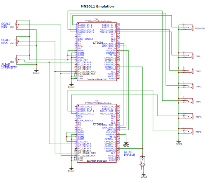
Program 5 : MN3011 Emulation
This program emulates the delay structure of the MN3011 BBD device.
|
Program 5 Pin Usage |
||||
|
Pin # |
Pin Name |
Primary Module |
Secondary Module |
Notes |
|
1 |
|
Audio Input 1 |
Unused |
|
|
2 |
|
Unused |
Unused |
|
|
46 |
|
Unused |
Unused |
|
|
45 |
|
Unused |
Unused |
|
|
3 |
|
Tap #4 output |
Tap #6 output |
|
|
4 |
|
Tap #3 output |
Tap #5 output |
|
|
46 |
|
Tap #2 output |
Unused |
|
|
45 |
|
Tap #1 output |
Unused |
|
|
20 |
|
Unused |
Unused |
|
|
19 |
|
Unused |
Unused |
|
|
18 |
|
Unused |
Unused |
|
|
17 |
|
Alias intensity |
Unused |
When OPTION_5=0 |
|
22 |
|
Global Delay Min |
Global Delay Min |
Primary/Secondary tied |
|
21 |
|
Global Delay Max |
Global Delay Max |
Primary/Secondary tied |
|
34 |
|
Unused |
Unused |
|
|
33 |
|
Unused |
Unused |
|
|
32 |
|
Unused |
Unused |
|
|
31 |
|
Unused |
Unused |
|
|
30 |
|
Aliasing |
Unused |
1=Disabled, 0=Enabled |
|
35 |
|
Unused |
Unused |
|
|
41 |
|
Unused |
Unused |
|
This program emulates the 6-output delay structure of the MN3011 BBD delay chip. To use the full 6-output capability of this program requires two CT3680 modules chained together (see Chaining Multiple Modules on page 49). If only a single module is used, this program will produce the first 4 outputs of the MN3011.
The 48kHz sampling rate must be selected when using this program (see Sampling Rate Selection on page 14).
This program supports aliasing (see Aliasing Feature on page 44). Only the manual aliasing mode is supported. To have consistent aliasing effects on all outputs, only the PRIMARY module of a 2-module configuration should have aliasing enabled. (Since output 1 of the PRIMARY is the input to the SECONDARY, it will already have aliasing distortion, so no additional aliasing is needed in the SECONDARY module).
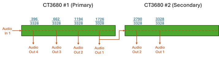
MN3011 emulation is achieved by fixing the CT3680 delay output ratios to the delay intervals of the physical MN3011 BBD chip. The 48kHz sampling rate must be selected for accurate MN3011 emulation. The following diagram shows the delay times as a percentage of the maximum, based on the physical hardware of the MN3011 BBD design. The MN3011 is a 3328 stage BBD. Output #1 of an MN3011 is at stage 396, so the delay at that point is 396/3328 = 0.11899 (11.9%). Output 2 is at stage 662, output 3 at 1194, output 4 at 1726, output 5 at 2790, and output 6 is at the last stage 3328.
Those delay time ratios are scaled into the global MIN/MAX delay times as set by their respective CV values. When two modules are used for the 6-output configuration, the MIN/MAX inputs of the two modules must be tied together (e.g. both modules get identical MIN/MAX CVs). This is in addition to the connections required for all module chaining configurations as described in the Chaining Multiple Modules section. If only a single module is used it will produce the first 4 output intervals, and no special hardware configuration is required.
If the aliasing feature is used with this program, the OPTION_5, and VC_DELAY_4 (alias intensity) of only the PRIMARY modules should be used.
Since the delay intervals are fixed, the VC_DELAY_1/2/3 inputs of both modules are unused. All the output delays are determined by mapping the MN3011 intervals into the MIN/MAX global range. The first 4 outputs are produced by the first (primary) module on AUDIO_OUT_4/3/2/1 (e.g. the shortest MN3011 delay is produced on AUDIO_OUT_4 of the first module, the 2nd shortest on AUDIO_OUT_3, the 3rd on AUDO_OUT_2, and the 4th delay is on AUDIO_OUT_1). The last 2 delays are produced by the second module on AUDIO_OUT_2/1 (5th delay on AUDIO_OUT_2 and the longest delay (6th) on AUDIO_OUT_1). Audio outputs 3 and 4 of the second module are unused.
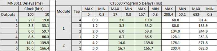
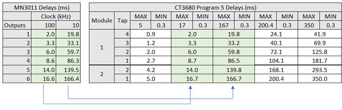
The CT3680 MN3011 emulation supports delay intervals over a wider range than the physical MN3011. At its maximum and minimum clock speeds the MN3011 supports delay taps from 2.0-16.6ms (at 100kHz clock) and 19.8-166.4ms (at 10kHz clock). The CT3680 supports delay ranges from 0.3-350ms. The following table shows some typical MIN/MAX settings and the resulting delay times for each output. For reference, the MN3011 delay times at minimum and maximum clock rates are also shown.
This program does not support the Tap Tempo feature.
Program 6 : MN300X BBD Emulations
This program provides emulation of nearly every model of BBD chip, including many that are no longer manufactured.
|
Program 6 Pin Usage |
|||
|
Pin # |
Pin Name |
Function |
Notes |
|
1 |
|
Audio Input 1 |
|
|
2 |
|
Audio Input 2 |
|
|
46 |
|
Audio Input 3 |
|
|
45 |
|
Audio Input 4 |
|
|
3 |
|
Chan 1 Output |
|
|
4 |
|
Chan 2 Output |
|
|
46 |
|
Chan 3 Output |
|
|
45 |
|
Chan 4 Output |
|
|
20 |
|
Unused |
|
|
19 |
|
Unused |
|
|
18 |
|
Unused |
|
|
17 |
|
Unused |
|
|
22 |
|
Alias intensity |
When OPTION_5=0 |
|
21 |
|
Unused |
|
|
34 |
|
Bit 0 |
Variation (BBD model selection) |
|
33 |
|
Bit 1 |
|
|
32 |
|
Bit 2 |
|
|
31 |
|
Unused |
|
|
30 |
|
Aliasing |
1=Disabled, 0=Enabled |
|
35 |
|
Unused |
|
|
41 |
|
Unused |
|
This program provides emulation of many different BBD chips including all MN30XX models MN3001-MN3010 (see Program 5 for MN3011), plus SAD512/SAD1024, TDA1022, and V3205, V3207, V3208. This program provides 4 independent delay lines, one for each audio input/output pair. Each line will emulate one of the BBD chips based on the variation selected. See Variation Selection below.
The 48kHz sampling rate must be selected when using this program (see Sampling Rate Selection on page 14).
Emulation consists of setting fixed minimum and maximum delay times based on the BBD datasheets. Since the min/max delay time is defined by the BBD model, the global VC_DELAY_MIN and VC_DELAY_MAX values are not used. Each of the four VC_DELAY_X inputs define the delay of a particular channel within the range defined by the BBD model. For example, a delay line configured for an MN3009 will have a minimum delay of 0.64ms (VC_DELAY_X at 0.0V) and maximum of 12.8ms (VC_DELAY_X at 3.3V).
Variation Selection
Variations define which BBD chips are emulated on which delay channel. 4 BBDs can be emulated at a time, in combinations defined by the variation.
1 of 8 variations can be chosen by the OPTION_1, OPTION_2, and OPTION_3 inputs. These form a binary number which selects one of the variations (see table below). Each variation emulates 4 BBD chips with each BBD on an independent delay line. For example, when variations zero is selected (OPTION pins 3,2,1 = LOW) delay channel 1 emulates an MN3003, channel 2 is an MN3006, channel 3 is an MN3007, and channel 4 is an MN3008.
Variations 0 through 4 define various combinations designed to provide a wide variety of delay lines. All BBD models are represented in at least one of the variations. Variations 5 through 7 provide dual delay lines of 2 selected types useful for stereo applications.
The following table shows which BBDs (and associated delay times) are on which channels for each of the 8 variations. To see which BBDs are in a particular variations, read one column of the table. Min and max delay times are in msec.
|
|
|
Variations selected by OPTION pins [3:2:1] |
|||||||
|
|
|
0 |
1 |
2 |
3 |
4 |
5 |
6 |
7 |
|
CHAN 1 |
BBD |
MN3003
|
MN3009
|
MN3006
|
MN3009
|
MN3006
|
MN3006
|
MN3001 |
MN3009
|
|
Min |
*0.16 |
0.64 |
0.32 |
0.64 |
0.32 |
0.32 |
0.32 |
0.64 |
|
|
Max |
3.20 |
12.80 |
6.40 |
12.80 |
6.40 |
6.40 |
25.60 |
12.80 |
|
|
CHAN 2 |
BBD |
MN3006
|
MN3001 |
MN3004 |
MN3007
|
V3207
|
MN3006
|
MN3001 |
MN3009
|
|
Min |
0.32 |
0.32 |
2.56 |
5.12 |
2.56 |
0.32 |
0.32 |
0.64 |
|
|
Max |
6.40 |
25.60 |
25.60 |
51.20 |
51.20 |
6.40 |
25.60 |
12.80 |
|
|
BBD |
MN3007 |
SAD512 |
V3207
|
MN3008 |
MN3005 |
MN3007
|
MN3008 |
MN3005 |
|
|
Min |
5.12 |
*0.17 |
2.56 |
10.24 |
20.48 |
5.12 |
10.24 |
20.48 |
|
|
Max |
51.20 |
170.67 |
51.20 |
102.40 |
204.80 |
51.20 |
102.40 |
204.80 |
|
|
CHAN 4 |
BBD |
MN3008 |
MN3005 |
MN3008 |
TDA1022
|
MN3005 |
MN3007
|
MN3008 |
MN3005 |
|
Min |
10.24 |
20.48 |
10.24 |
51.20 |
20.48 |
5.12 |
10.24 |
20.48 |
|
|
Max |
102.40 |
204.80 |
102.40 |
512.00 |
204.80 |
51.20 |
102.40 |
204.80 |
|
(*) BBDs with a min delay < 0.3ms will have an emulated min delay = 0.3ms (MN3003 and SAD512).
Aliasing
This program supports the Aliasing Feature as described on page 45. Aliasing is controlled by VC_DELAY_MIN (which is otherwise unused in this program). This program supports both manual mode and automatic mode aliasing. Mode is selected by the value of the VC_DELAY_MIN control voltage:
· 0.0v-3.0v is automatic mode
· 3.0v-3.3v is manual mode.
Manual mode (VC_DELAY_MIN between 0.0V and 3.0V) operates as described in the Aliasing Feature section – 0.0V results in no aliasing distortion, values near 3.0V result in maximum aliasing (simulating a sample rate approaching zero).
Automatic mode (VC_DELAY_MIN >= 3.0V) the amount of aliasing is automatically determined by the characteristics of the simulated BBD and the current delay setting. This is done by determining the BBD clock speed that corresponds to the current delay setting for the simulated BBD and applying aliasing that corresponds to that clock speed. If the determined clock speed is >48kHz then no aliasing is applied.
For example, if an MN3007 is being simulated (variation 3, channel 2) and the VC_DELAY_2 input is set to 2.8V, then the delay of channel 2 will be 44.2ms1F[2]. In a real MN3007 BBD chip, this would occur at a clock speed of 23.6kHz2F[3]. In automatic mode an aliasing effect corresponding to 23.6kHz would be applied to channel 2. If the delay CV is changed, then the corresponding aliasing level automatically changes to track it.
Programs 7 and 8 : Multi-Effects
 |
These programs support tap tempo and optional aliasing effects. I/O pin usage for these programs are summarized in the following table. The function of many of the pins are determined by which variation is selected within the program.
|
Program 7 and 8 Pin Usage |
|||
|
Pin # |
Pin Name |
Function |
Notes |
|
1 |
|
Audio Input 1 |
Assignment of inputs and outputs are defined by the selection of Variation |
|
2 |
|
Audio Input 2 |
|
|
46 |
|
Audio Input 3 |
|
|
45 |
|
Audio Input 4 |
|
|
3 |
|
Audio Output 1 |
|
|
4 |
|
Audio Output 2 |
|
|
46 |
|
Audio Output 3 |
|
|
45 |
|
Audio Output 4 |
|
|
20 |
|
Delay Control 1 |
Use of VC_DELAY inputs is defined by the selection of Variation |
|
19 |
|
Delay Control 2 |
|
|
18 |
|
Delay Control 3 |
|
|
17 |
|
Delay Control 4 |
|
|
22 |
|
Long chan aliasing intensity |
When OPTION_5=0 |
|
21 |
|
Short chan aliasing intensity |
When OPTION_5=0 |
|
34 |
|
Bit 0 |
Selects 1 of 8 tap tempo dividers |
|
33 |
|
Bit 1 |
|
|
32 |
|
Bit 2 |
|
|
31 |
|
Variation selector |
1=select variation A, 0=select variation B |
|
30 |
|
Aliasing |
1=Disabled, 0=Enabled |
|
35 |
|
Tap tempo switch input |
|
|
41 |
|
Tap tempo LED output |
|
The VC_DELAY_MAX/MIN inputs are not used for global scaling in this program, the delay time of each output is only controlled by a single VC_DELAY control input. The assignment of VC_DELAY control to specific outputs is determined by the selected program/variation (see variation descriptions below).
The maximum delay time depends on the type of channel and the sampling rate (the minimum delay of all channels is 0.3ms). This table shows the general range of maximum delay times by channel type and sample rate. The exact maximum delay time for each channel is given in the Program/Variations section.
|
Channel Type |
Maximum Delay (ms) |
|||
|
48kHz |
32kHz |
24kHz |
12kHz |
|
|
Extended |
576-612 |
864-918 |
1152-1224 |
2304-2448 |
|
Long |
305-340 |
457-510 |
610-680 |
1220-1360 |
|
Short |
35 |
35 |
35 |
35 |
Long and Extended Type Channels
Long and Extended channels have the same features; the only difference is the general range of maximum delay time. Extended channels have a maximum delay of ~600ms whereas Long channels have a maximum delay of ~330ms (at 48kHz). See the Program/Variations section for exact delay times available.
Long and Extended channels have 1 input and 1 (“Single”) or 2 (“Dual”) outputs. Each output is an independently controlled delay of the input.
The tap tempo feature works differently for SINGLE and DUAL channels:
For SINGLE channels, the tap interval sets the maximum delay time of the channel. The channel CV_DELAY control then determines the actual delay time as usual (e.g. the full CV range varies the delay time from 0.3ms to the tap interval). The tap interval is determined by dividing the physical tap time by one of 8 musical intervals as selected by the OPTION_1,2,3 pins:
|
OPTION inputs [3,2,1] |
Channel max delay is set to this fraction of tap time |
Musical interval |
|
[000] 0 |
1/16 |
Sixteenth |
|
[001] 1 |
1/8 |
Eighth |
|
[010] 2 |
1/8+1/16 |
Dotted Eighth |
|
[011] 3 |
1/4 |
Quarter |
|
[100] 4 |
1/4+1/8 |
Dotted Quarter |
|
[101] 5 |
1/3 |
Third |
|
[110] 6 |
1/2 |
Half |
|
[111] 7 |
1 |
Whole |
For DUAL channels the CV_DELAY controls are ignored, and the output delay is determined solely by the tap interval and the selected tap divider (OPTION_1,_2,_3 pins). The delays of the 2 outputs of the channel are set to musically related intervals (see Tap to Dual Intervals section on page 44).
When aliasing is enabled by OPTION_5 (LOW), aliasing on all Long/Extended channel outputs are controlled by the VC_SCALE_MIN input. A value of 0.0V will produce outputs with no aliasing, and a value of 3.0V will produce maximum aliasing. All Long/Extended outputs will always have the same amount of aliasing effect.
Short Type Channels
Each “Short” type channel has 1 input and 1 output with the delay set by one of the VC_DELAY_x control voltages. Short channels always have a maximum delay of 35ms no matter what sample rate is selected.
The short channel delay time is set by a single VC_DELAY control input. The assignment of VC_DELAY control to specific outputs is determined by the selected variation (see variation descriptions below). The delay time of a short channel is not affected by tap tempo or the VC_MIN_DELAY and VC_MAX_DELAY control inputs.
When aliasing is enabled by OPTION_5 (LOW), aliasing on the Short channel output is controlled by the VC_SCALE_MAX input. A value of 0.0V will produce no aliasing effect, and a value of 3.0V will produce maximum aliasing.
Programs/Variations
Programs 7 and 8 each support 2 “variations”, which defines how many Extended, Long and Short channels there are, how many outputs for each channel (“Single” or “Dual”), and which physical inputs and outputs are assigned.
The program/variations are defined to provide different combinations of long and short delay channels to allow building of various multi-delay combined effects. There is also consideration for linking multiple CT3680 modules together with these program/variations to provide longer echo delays and more flexibility.
The programs/variations are summarized below, and the following sections describe each one in more detail:
|
Program/Variation |
OPTION_4 |
Chan 1 |
Chan 2 |
Chan 3 |
Chan 4 |
|
7/A |
1 (HIGH) |
Extended Dual |
Short |
Short |
- |
|
7/B |
0 (LOW) |
Long Dual |
Long Dual |
- |
- |
|
8/A |
1 (HIGH) |
Long Single |
Long Single |
Short |
Short |
|
8/B |
0 (LOW) |
Extended Single |
Short |
Short |
Short |
Program 7 Variation A
Program: 7
OPTION_4: HIGH
This variation configures the module with 1 Extended Dual, and 2 Short channels.
|
Channel |
Type |
Outputs |
Maximum Delay (ms) |
|||
|
48kHz |
32kHz |
24kHz |
12kHz |
|||
|
1 |
Extended |
Dual |
612 |
918 |
1224 |
2448 |
|
2 |
Short |
Single |
35 |
35 |
35 |
35 |
|
3 |
Short |
Single |
35 |
35 |
35 |
35 |
Input/output assignments and VC_DELAY control usages are shown here:
Program 7 Variation B
Program: 7
OPTION_4: LOW
This variation configures the module with 2 Long Dual channels.
|
Channel |
Type |
Outputs |
Maximum Delay (ms) |
|||
|
48kHz |
32kHz |
24kHz |
12kHz |
|||
|
1 |
Long |
Dual |
340 |
510 |
680 |
1360 |
|
2 |
Long |
Dual |
340 |
510 |
680 |
1360 |
Input/output assignments and VC_DELAY control usages are shown here:
Program 8 Variation A
Program: 8
OPTION_4: HIGH
This variation configures the module with 2 Long Single, and 2 Short channels.
|
Channel |
Type |
Outputs |
Maximum Delay (ms) |
|||
|
48kHz |
32kHz |
24kHz |
12kHz |
|||
|
1 |
Long |
Single |
305 |
458 |
610 |
1220 |
|
2 |
Long |
Single |
305 |
458 |
610 |
1220 |
|
3 |
Short |
Single |
35 |
35 |
35 |
35 |
|
4 |
Short |
Single |
35 |
35 |
35 |
35 |
Input/output assignments and VC_DELAY control usages are shown here:

Program 8 Variation B
Program: 7
OPTION_4: LOW
This variation configures the module with 1 Extended Single, and 3 Short channels.
|
Channel |
Type |
Outputs |
Maximum Delay (ms) |
|||
|
48kHz |
32kHz |
24kHz |
12kHz |
|||
|
1 |
Extended |
Single |
576 |
864 |
1152 |
2304 |
|
2 |
Short |
Single |
35 |
35 |
35 |
35 |
|
3 |
Short |
Single |
35 |
35 |
35 |
35 |
|
4 |
Short |
Single |
35 |
35 |
35 |
35 |
Input/output assignments and VC_DELAY control usages are shown here:
Tap Tempo Feature
Some programs support the ability to set delay times based on user input ‘tapping’. Typically, this is done by a momentary switch connected between the TT pin (35) and GND. The user taps once to start a delay interval, and a second time to denote the end of the interval. This puts the CT3680 in tap-tempo mode and that interval (from first tap to second tap), is then used to set delay times in various ways as described in the following sections. Pressing and holding the switch for 1 second clears tap-tempo mode and delays are then defined as usual by the CV inputs.
When tap tempo mode is engaged, the TT_FLASH output pin (41) can be used to drive an LED that will flash at the tap interval rate (hardware revision 2.1 or later, see PCB Design Notes on page 55).
In general, tap tempo is useful only for effects that user longer delay times as it is difficult for a user to tap quickly enough to accurately set short delay times.
Programs that support tap-tempo use one of two methods to apply the tap interval to delay times. See the individual program descriptions to know which method is used by which programs. The tap-tempo methods are:
Tap to Max
The “tap to max” method applies the tap interval directly to the global MAX delay scalar, overriding the VC_SCALE_MAX input[4]. This method also sets the global MIN scalar to zero. The result is the same as setting the VC_SCALE_MIN input to 0.0v, and the VC_SCALE_MAX input to correspond to the tap interval (or a fraction of it as defined by OPTION pins, see below). For most programs this alters the delay range for all channels and all outputs to be 0ms to the tap interval (ms). See Global Scalars on page 48 for details on how the MIN/MAX global scalars affect delay times.
Often it is useful to allow the user to tap to a music beat but set the delay to a fraction of that interval. E.g. if the music is 60bpm (1 beat per second) it is easy to tap that interval, but it may be desirable to set the delay to a musical sub-interval of 1 second. OPTION inputs 1, 2, and 3 form a binary number used to select a sub-interval of the tap time to be applied to the MAX scalar. The following table shows the 8 possible OPTION settings and the corresponding musical interval:
|
OPTION inputs [3,2,1] |
MAX scalar is set to this |
Musical interval |
|
[000] 0 |
1/16 |
Sixteenth |
|
[001] 1 |
1/8 |
Eighth |
|
[010] 2 |
1/8+1/16 |
Dotted Eighth |
|
[011] 3 |
1/4 |
Quarter |
|
[100] 4 |
1/4+1/8 |
Dotted Quarter |
|
[101] 5 |
1/3 |
Third |
|
[110] 6 |
1/2 |
Half |
|
[111] 7 |
1 |
Whole |
If the calculated MAX interval exceeds the maximum possible delay time of a
channel, the delay time is set to the maximum possible for that channel.
Note that OPTION[3,2,1]=7 applies the tap interval directly to the MAX scalar.
Tap to Dual Intervals
The “dual intervals” tap method is used in some programs that have a long-delay channel with 2 outputs. This method produces two musically related delay intervals on the outputs of the channel to which it is applied (see the program descriptions for how this method works in programs that support Tap to Dual Intervals).
When the user taps an interval the two outputs of the affected channel are set to the following fractional delay times:
|
OPTION inputs [3,2,1] |
Delay (fraction of tap time) |
Effect |
|
|
Output 1 |
Output 2 |
||
|
[000] 0 |
1/4 |
1/8 + 1/16 |
Rhythmic delay with a bit of syncopation |
|
[001] 1 |
1/4 |
1/8 |
Steady rhythmic echo with additional repeats btw 1/4 notes |
|
[010] 2 |
1/2 |
1/4 |
Longer spacious delay with synchronized repeats |
|
[011] 3 |
1/4 |
1/6 |
Swinging triplet feel |
|
[100] 4 |
1/4 |
1/16 |
Quick repeats between 1/4 notes for staccato effect |
|
[101] 5 |
1/4 + 1/8 |
1/8 |
Complex alternating rhythmic pattern |
|
[110] 6 |
1/2 |
1/8 |
Longer delay with very quick repeats |
|
[111] 7 |
VC_DELAY_1 |
VC_DELAY_2 |
Arbitrary delays from 0ms to tap interval, set with CV inputs |
When the user taps the beat interval and these dual delays are mixed together, they produce rhythmic echo patterns based on the selected OPTION inputs.
Any VC_DELAY control inputs that would normally define the delay times of these outputs are disabled while tap tempo is engaged except when OPTION 7 is selected. When the OPTION inputs are set to 7 [111] the delay times are defined by the VC_DELAY voltage scaled into the range 0ms to the tap interval. E.g. a VC_DELAY input of 0.0v will produce a delay of 0ms, and an input of 3.3v will produce a delay equal to the tap interval. This allows arbitrary dual delay intervals to be defined. For example, if it was desired to have 1/3 and 1/6 echoes (for which there is no OPTION setting), set option pins to 7 [111] and
![]()
and
![]()
would produce the desired fractional delayed outputs. E.g. with OPTION[3:1] set to [111] and VC_DELAY_1 set to 1.1v, and VC_DELAY_2 set to 0.55v, then the delay outputs 1 and 2 will 1/3 and 1/6 of the tap interval respectively. If a calculated tap delay exceeds the maximum delay for that channel, the maximum will be used instead.
Note that which VC_DELAY input controls which output is defined by the selected program. Use of VC_DELAY_1 and 2 above is just for illustration, see the individual program descriptions.
Aliasing Feature
When the CT3680 is run at the default 48kHz sampling rate it does not have any audible aliasing effect at any delay time; the output is a clean, accurate, low-distortion delayed copy of the input. However, designers interested in delay-based effects that “sound like” classic BBD chips may find the CT3680 sound too clean and artifact-free for the sonic effect they desire. BBD chips introduce aliasing distortion at longer delay times because the longer times are achieved by slowing the sampling rate. The CT3680 does not naturally have this aliasing distortion effect because long delay times are not achieved by changing the sampling rate. If aliasing distortion is desirable in a CT3680-based effect, the CT3680 can emulate BBD-like aliasing distortion with the feature described here.
The effect of this “Aliasing Feature” should not be confused with aliasing caused by running the CT3680 at lower sampling rates. As of version 2.0 of the hardware, it is possible to select sampling rates below the default 48kHz (specifically 32kHz, 24kHz, and 12kHz). When those lower rates are used some amount of aliasing distortion will be introduced in all outputs, independently of this Aliasing Feature. At 32kHz such aliasing distortion is minimal, at 24kHz it may become noticeable in the higher audio frequences, and at 12kHz it is quite noticeable except in the bass regions. If this Aliasing Feature is used with one of the lower sampling rates (32, 24, or 12kHz) it will add a variable amount of distortion to the inherent aliasing caused by the lower sampling rate. E.g. the aliasing effect of lower sampling rates and the aliasing effect of this feature are additive.
Some programs have an Aliasing Feature which can be enabled with an OPTION pin. As described above, this feature emulates the behavior of physical BBD devices when they are run at lower clock speeds (e.g. longer delay times). Aliasing is a form of distortion caused by sampling the audio at a rate lower than 2 times the maximum audio frequency. Some BBD-based systems use the aliasing distortion as part of the intended effect and consider it desirable, and in some way “authentic” to classic BBD delay sound.
The aliasing feature of the CT3680 allows the effects designer to choose how much, if any, aliasing distortion is to be introduced into the output signal, and to control it in various ways. By disabling this effect (the default state) and running the CT3680 at the 48kHz sampling rate, a “clean” delay is produced with no audible aliasing. This feature should only be used if the circuit designer specifically desires some level of aliasing distortion.
In a physical BBD device, the intensity of the aliasing changes with the delay time (since delay time is defined by (clock) sampling rate). Longer delay times produce a high intensity (more distortion). The Aliasing Feature of the CT3680 can be used to simulate the aliasing effect of any sampling rate and it can be varied (modulated) with delay time or in some other way via a CV input.
The OPTION_5 pin enables aliasing mode when it is set LOW (for programs that support this feature). This pin has an internal pull-up resistor, so if left unconnected aliasing is disabled.
|
OPTION_5 |
Aliasing Effect |
|
N.C. |
Disabled |
|
HIGH |
Disabled |
|
LO |
Enabled |
The intensity and mode of the aliasing effect can be controlled by one of the VC inputs (which CV input is used to control aliasing is defined by the selected program – see the program descriptions). Control of the aliasing can be manual mode or automatic mode. The mode is determined by the CV input voltage range. When the CV is between 0.0V and 3.0V the aliasing is in manual mode. When the CV is 3.0 to 3.3V aliasing is automatic. Note that not all program support both modes, see the program descriptions.
Manual Mode Aliasing
Manual mode is selected with an aliasing effect VC voltage in the range 0.0V to 3.0V. The intensity is set by the value of the VC input such that an input voltage of 0.0V will cause no effect and an input voltage of 3.0V will simulate a sampling rate approaching zero (maximum aliasing distortion). The aliasing effect CV input can be set to any level of desired aliasing, or it can be varied over time or in sync with the delay settings. It must remain in the range of zero to 3.0V for manual mode control.
When manual aliasing is at its most extreme setting (approaching 3.0V) this can cause the audio to drop out because the output signal approaches DC (constant value) which is then filtered out by the CT3680 a/c coupled outputs.
Automatic Mode Aliasing
Automatic mode aliasing is selected when the aliasing effect CV input is above 3.0V (e.g. 3.0V to 3.3V). In automatic mode the intensity of the aliasing is automatically determined by the delay settings to simulate real BBD hardware in which the aliasing effect is more intense at longer delay times. See the individual program descriptions for how automatic aliasing intensity is determined. If the program does not support automatic aliasing, then alias effect CV inputs above 3.0V have the same effect as 3.0V (e.g. maximum manual aliasing).
If multiple modules are chained together, in general it is desirable that they all produce the same aliasing effect (although it is not required). To achieve that, the OPTION_5, and aliasing effect VC input of all modules in the chain should be tied together. See the Chaining Multiple Modules section on page 49.
Setting Delay Times
Delay CV Inputs
Delay times in the CT3680 are defined by CV (control voltage) inputs in the range of 0.0v to +3.3v. A minimal CV input (0.0V) indicates a minimum delay time, and a maximum CV input (+3.3V) indicates a maximum delay time. CV values between 0.0V and 3.3V define a linear scaling of delay time between the minimum and the maximum. What actual delay times those represent depends on the global delay scalars (see next section), the currently selected program (see Program Selection on page 15), and the currently selected sampling rate (see Sampling Rate Selection on page 14). The CT3680 is capable of delay times from 0.3ms to 2.7 seconds.
Exponential Scaling
PREVIEW FEATURE
By default, delay times are calculated on a linear scale between 0.0v and 3.3v. For example, a control voltage of one half the maximum (3.3 / 2 = 1.65v) would create a delay time half way between the MIN and MAX (see the red line in the graph below). The linear delay time is calculated as:
![]()
When exponential scaling is enabled, the delay is calculated as:
![]()
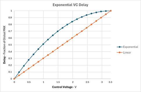
The effect of exponential scaling is that delay time is more sensitive to VC changes at small delay times, and less sensitive at large delay times. This can produce a more nature delay modulation effect particularly when the modulation waveform is a triangle.
Global Scalars
Most programs support the use of two CV inputs (VC_SCALE_MIN, VC_SCALE_MAX) define a global range for all delay times (see Summary of Programs on page 15 to see which programs support this feature). All individual delays on all channels are scaled to be in the range of MIN-MAX. This allows individual delay CV inputs to use their full scale (0.0V to 3.3V) to cover a range of delay values that are of use for a particular application. With a narrower global range, the CV delay inputs operate with more precision in the delay range of interest and makes them less susceptible to noise.
For example, if a module is to operate as a 2 channel delay with delay times between 100ms and 200ms, then program 1 would be selected since it defines a 2 channel configuration. The table in the Program Selection section shows the maximum delay time for that program is 341ms at 48kHz sampling rate. To set a global minimum delay to 100ms, the VC_SCALE_MIN would be set to:
![]()
To set a global maximum of 200ms, VC_SCALE_MAX would be set to
![]()
With those settings, both delay channels are constrained to a minimum delay of 100ms, and a maximum delay of 200ms.
With those global MIN/MAX settings, the CV delay inputs (VC_DELAY_x) used to set the individual output delay times have a full scale range of 100ms to 200ms. E.g. setting VC_DELAY_1 to 0.0v would result in channel 1 output 1 (on pin AUDIO_OUT_1) to be delayed 100ms (global MIN). Setting it to its halfway point (3.3/2=1.65v) would result in a delay time halfway between global MIN and MAX, e.g. 150ms. Setting it to full scale 3.3v results in a delay time of 200ms (global MAX). Global MIN and MAX delays are always calculated on a linear scale.
The global MIN and MAX times apply to all channels and all outputs unless otherwise noted in the program description.
The global MIN and MAX delay time CV inputs are really a differential pair. It is not required that VC_SCALE_MAX be greater than VC_SCALE_MIN. The lower of the two CVs defines the global minimum delay time and the higher of the two defines the global maximum delay time. If the values are the same, then all delays are constrained to that single value.
All CV inputs, including the global scalars, may be modulated (varied with time) to achieve various effects.
Chaining Multiple Modules
Overview
This feature allows multiple modules to be (digitally) chained to achieve longer delay times and/or more outputs without signal degradation. The limit of how many modules can be chained depends on the integrity of the shared bus signals but 5 modules should be chainable with no additional hardware.
Chained modules are defined by a single Primary module (the PRIMARY input pin is HIGH) and some number of downstream Secondary modules (with the PRIMARY input pin pulled LOW). There can be only a single primary module in a linked system. LINK signals must be connected between the modules as described in this section. A primary module copies its AUDIO_OUTPUT_1 to the Secondary module’s AUDIO_INPUT_1. This is a digital copy so chaining multiple modules does not degrade the audio quality. The Primary module’s analog output 1 is still active and can be used as a delay output as usual. The secondary’s analog input 1 is not used. If desired, 2 channels can be linked by tying the LINK_1CH input pin low on the secondary module. When that pin is LOW, outputs 1 and 2 of the Primary are copied to inputs 1 and 2 of the secondary.
(Need diagram here showing channel 1,2 linking)
The sampling rate selected on the Primary module will be used on all Secondary modules. Secondary module RATE_0 and RATE_1 input pins are ignored.
There are many possible uses for module chaining. In the simplest case, it can be used to achieve a longer overall delay time than the maximum delay of a single module. For example, a delay time of 750ms (3/4 sec) at 48kHz exceeds the total delay time of a single module. To achieve 750ms delay, a 2-module chain could be used, the first module in the chain could implement a delay with Program 0 and set outpu1 1 delay time to 500ms. The first (primary) module output 1 output is copied to input 1 of the second module via the digital chain. If that module is also running Program 0, then it can add up to 682ms additional delay (it will also be sampling at 48kHz). By setting the MIN/MAX scalars and delay CV signals appropriately, it could add 250ms delay to its output #1 , thus achieving a 750ms delay from input 1 to the first module, to output 1 of the second.
Another use of chaining is to achieve more delay outputs than the 4 outputs supported by a single module. More outputs allow for a richer variety of delayed signals to mix, filter and process. Program 5 (MN3011 emulation) uses 2 modules to emulate the 6 outputs of the MN3011 BBD chip.
Cumulative Delay
Because downstream modules read their input 1 (and possibly input 2) from upstream (delayed) outputs, delay is cumulative from module to module down the chain. Note that each module is always limited (by program selection) in the total amount of delay it can add, and that if a module changes the delay of output #1, that change propagates to all downstream modules. Since each module can be running a different Program, a wide variety in number of delay channels and total delay times can be achieved. Chaining is always limited to passing 1 or 2 audio outputs from one module to the next.
AUDIO_OUT_1 of the upstream modules is copied to input 1 of the downstream module (and possibly output 2 to input 2), but all the analog outputs of the upstream module (including analog outputs 1 and 2) are active and behave according to the selected program. Also note that if a downstream program defines multiple delay channels, only the channel driven from input 1 (and possibly 2) receives data from the upstream module; all other channels of the downstream module run independently within that module and may process completely independent audio signals.
Hardware Configuration
To achieve chaining, one module is designated as the Primary module, all others are Secondary modules. All modules in the chain must be connected by their LINK_BUS_1 and LINK_BUS_2 pins. On each upstream/downstream pair, the upstream LINK_OUT must be connected to the downstream LINK_IN. These are digital signal lines so PCB layout should be done accordingly. All modules should share a common ground and power supply.
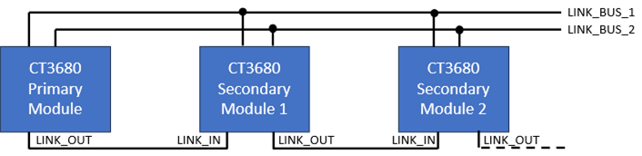
When modules are chained together, the PRIMARY module pin is held HIGH (or unconnected), all others (the Secondary modules) must have the PRIMARY pin held LOW.
All secondary modules disable their analog AUDIO_IN_1, and audio is instead copied (digitally) from AUDIO_OUT_1 of the nearest upstream module. Depending on the program selected in the downstream module, other analog audio inputs may be active. Module audio chaining is always AUDIO_OUT_1 of the upstream module to AUDIO_IN_1 of the downstream module (and AUDIO_OUT_2 to AUDIO_IN_2 when 2-channel linking is enabled via the LINK_1CH input pin). AUDIO_OUT_1 and AUDIO_OUT_2 may also be used as a normal analog outputs on any of the modules of the chain.
It is also possible for a Primary (or any upstream) module to drive multiple downstream modules, copying its output(s) to the input(s) of more than one downstream module. In this example, the Primary module output 1 is digitally copied to the input 1 of both modules 1a and 1b.
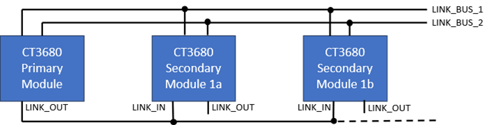
The topology can mix single and multiple downstream modules in a system, but there can be only 1 Primary module, and no more than 5 total.
Chained Programs
Each module in the chain selects its program setting with its own set of PGM input pins (see Program Selection on page 15). It is not required that every module run the same program but note that AUDIO_INPUT_1/2 is disabled on all downstream modules, programs that read input 1 will instead read output 1 of the upstream module as their input. Some programs are designed for multi-modules configurations (e.g. Program 5, the MN3011 emulation program, and Program 7, multi-effects) in which case that program should be selected on all the modules.
In general, it is not required that global MIN/MAX scalars be linked between modules in any particular way. Modules in the chain may each have their own independent scalars, or a single CV can be used to drive the MIN/MAX on multiple modules. Other inputs may or may not be tied together depending on the application.
Typical Applications
Minimum Reference Schematic
This represents a minimum circuit to implement a 1 line, 4 output delay with manual (potentiometer) CV controls. For this configuration program 0 is selected (all PGM pins held LOW). The mixer here is conceptual, to show that the original (dry) signal and the various delayed signals might be mixed at various relative levels to produce a single audio output.
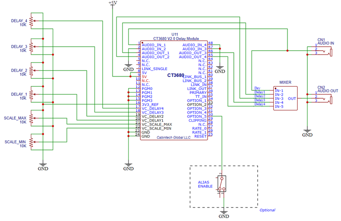
Primary/Secondary Linked Modules
This is a minimum circuit to implement an 8 input, 8 output delay system composed of two linked CT3680 modules with manual CV controls. Both modules should share a common ground and power supply. They may also have shared inputs such as the alias feature controls (OPTION_5, and a VC_DELAY input), depending on the application.
Note the secondary module has the PRIMARY pin tied to ground. Each module is shown with a jumper block to select the program for that module.
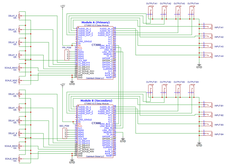
Physical Dimensions
Board dimensions: 38mm (1.5in) x 22mm (0.87in).
Edge pin pitch (spacing): 1.4mm (0.055in)
PCB Design Notes
When designing a PCB on which the CT3680 will be used, note the following guidelines:
1. External
LED outputs (Pin 41 tap tempo, and pin 29 clipping):
Hardware rev prior to 2.1C
a. These LED outputs are low-current (2mA max) that cannot directly drive an external an LED.
b. A
circuit like the following can be used to drive an LED. Adjust R2 as necessary
for the particular LED being used. Also note that the top of R2 could go to any
supply voltage, it does not have to take LED power from the CT3680 3.3V
reference supply.
Hardware rev 2.1C and later:
c. These
LED outputs can sink up to 0.8mA max, sufficient for many small modern LEDs. Be
sure to use a current limiting resistor to limit max current at 3.3V to 0.8mA
or less.
2. Adjacent +5 and GND pins should both be connected to the appropriate PCB traces. When possible, use larger track sizes for power and ground connections.
3. Any pin noted as “N.C.” in the Pinout section on page 10 should be left unconnected on the PCB. Do not tie these pins to power, ground, or each other.
4. It is recommended that a 3 pin header be included on the PCB that provides connections to pins 10, 11, and GND of the CT3680. These pins can be used to install firmware updates (see Firmware Updates on page 56). Pin 1 of the header should be connected to pin 11 (I2C_SDA) of the module, pin 2 is GND, and pin 3 should be connected to pin 10 (I2C_SCL). Production scale designs that are not intended to be updated can omit this header.
5. Schematic symbols, PCB footprints, 3D models, and other design resources are available on the Cabintech website. Symbols and footprints can help avoid errors in the schematic connections and PCB layout.
Firmware Updates
It is not common, but on occasion it may be useful to update the CT3680 firmware to obtain newly developed firmware programs or enhancements to existing programs. Updating the module firmware requires an FXCore In Circuit Programmer (ICP) board, available on our website. This board provides a bridge between a computer USB port and the CT3680 module. Currently this update process is supported only on Windows 10 or later.
Installing the Updater Application
To update a CT3680 module you will need to download the CT3680 updater application. This application requires:
- Windows 10 or later with
o Java 17 (or later) installed
o A modern web browser installed (Chrome, Edge, etc)
- A connection to the internet
The updater is a Windows executable that can be downloaded and run (no installer or unpacking necessary). Download the updater from:
https://cabintechglobal.com/appfiles/ct3680/ct3680-updaterui.exe
This file will be used to update the module in a later step.
Connecting to the Module
You will need access to 3 pins of the CT3680 module (I2C pins 10 and 11) and GND. It is recommended that PCB designs include a 3-pin header for this purpose. The I2C bridge adapter has 3 pins that must be connected to the CT3680. The adapter has markings indicating “SCL” (topmost pin in the photo below), “SDA” (bottom pin), and the center pin is GND. These pins of the adapter must be connected as follows:
|
ICP Adapter |
CT3680 |
|
Pin 3 (top pin) “SCL” |
|
|
Pin 2 (center pin) GND |
|
|
Pin 1 (bottom pin) “SDA” |
|
If the PCB on which the CT3680 is mounted has a 3-pin header with these signals, a simple 3-wire cable can be used to connect the adapter to the module. The CT3680 development board has such a header labeled “BURN” or “UPDT”.
Running the Updater
The updater will connect to the Cabintech update service to retrieve the updates and install them into the CT3680.
Before running the updater, verify:
1. The Windows PC is connected to the internet.
2. The CT3680 is powered through its normal power supply pins (the ICP will not supply power to the CT3680).
3. The ICP is connected by a USB cable to the Windows PC.
4. The ICP is connected to the CT3680 by a 3-pin cable as described above.
Run the updater as follows:
1. Execute
the ct3680-updaterui.exe program (downloaded in an earlier step) from
Windows File Explorer, from you browser download list, or a command-line
window. It can be executed in whatever directory in which it was downloaded.
It does not require administrator privileges.
You may get a warning message about an ‘unrecognized app’ or ‘unknown
publisher’ similar to these. If you do, click through them to allow the program
to run:
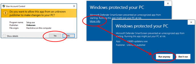
2. The updater will show a brief splash screen, then open a window (or tab) in your web browser. After downloading some required resources, the updater will attempt to read the attached CT3680 module and will then show details about the module and options to update it:
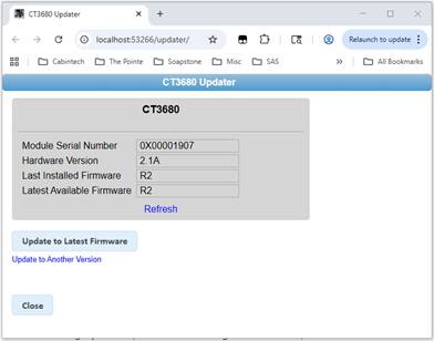
3. To update the module to the latest available firmware, just click the Update to Latest Firmware button. After a confirmation, the update process will start and the update progress will be shown:
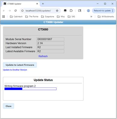
4. When
the update is complete the status will show “Update completed with no errors”
and the module details will be updated.
5. To exit the updater, click the Close button or close the browser tab.
Installing Alternate Firmware Versions
As described above, the updater will install the latest production release of the firmware. It is possible to install other versions as may be necessary for beta testing or when Cabintech supplies custom firmware for specific customers. Consult with us before using this option.
To install a non-standard version of the firmware, run the Updater program and instead of clicking on the Update to Latest button, select the “Update to Another Version” link below it:
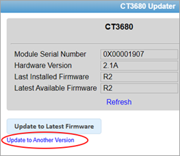
You will be prompted to enter the version to be installed, and then the update will proceed as usual.
Development / Breakout Board
A development board is available to aid in prototyping and development of CT3680 based products. The dev board makes all the inputs and outputs of the module accessible through header pins and connectors. The board has 6 potentiometers for manual CV control and switches for setting the program number, option inputs, and other settings. Audio inputs and outputs are available through standard TS (mono) 3.5mm jacks, as well as a TRS (stereo) connector that combines audio outputs 3 and 4. The dev board also has probe points for all pins of the module as well as headers for signals that may be processed off-board.
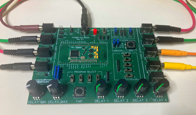
Development Board Features
· 6 potentiometers for CV controls
· 8 mono (TS) 3.5mm audio input/output jacks
· 1 stereo (TRS) 2.5mm audio output jack (combines outputs 3+4 into L+R)
· 4 program select switches
· 5 option select switches
· Tap-tempo momentary push button
· Controls for system sampling rate, multi-module configuration, and system reset
· Power connector jack
· Power on/off switch and LED
· Header pins for all audio inputs and outputs
· 5V, 3.3V, and GND header pins
· Headers for upstream and downstream linked modules
· Test points for all pins of the CT3680 module
Power Supply
The power section of the dev board has a 2.1mm power jack (center positive) for +5V power input, an ON/OFF switch, and a LED. The ON/OFF switch allows control of power to the board without removing the power plug. Double header pins are supplied for off-board access to 5V, 3.3V, and GND. When using multiple development boards it is handy to jumper the 5V supply and GND lines together so only one board needs to have a power plug. Do not tie 3.3V supplies of multiple boards together. Each board generates its own independent 3.3V supply via a regulator on the module.
Program Selection
The board has 4 program selection switches to allow setting the program via the module’s PGM pins. The program select lines are also made available on header pins so program selection can be controlled off-board (for example, by a microcontroller). When driving the program select lines off-board, the switches must remain in the LOW (off) position.
Option Selection
The board has 5 selection switches in the OPTIONS section that allow control of various program options. Header pins make option control available to an off-board controller. When driving the option pins off-board, the option switches must remain in the HI position.
System Settings
The SYSTEM section has 2 jumpers that select one of 4 sampling rates. The legend on the board shows the proper position of the jumpers for 48kHz, 32kHz, 24kHz, or 12kHz sampling rates. Note that sampling rate changes do not take effect until the system is reset or power cycled. There is a push button switch in the SYSTEM section to reset the module.
Delay (CV) Controls
The board has 6 potentiometers along the bottom edge for control of the min/max/1/2/3/4 delay parameters. At the full counterclockwise position, the CV voltage will be 0.0V, full clockwise is 3.3V. The potentiometers are linear. If CV is to be supplied off-board, the CV control jumpers should be removed, and the external CV signals should be supplied to the rightmost pins of the jumper block (closest to the program switches).
![]()
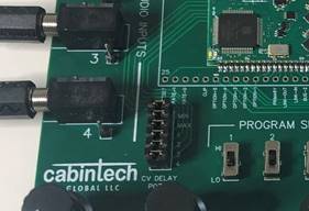
When driving the CV controls from off-board, the CV jumpers must be removed.
Audio Input/Output
3.5mm TS mono jacks are provided for the (4) audio input and (4) audio outputs of the CT3680 module. Each input and output also has a single header pin that is handy for clipping test leads. There is also a single TRS stereo output jack that combines audio outputs 3/4 into a left/right stereo pair.
Tap Tempo
The board has a momentary push button style switch along the front edge between the CV controls. When depressed this button shorts pin 38 (TT_IN) to ground. This button can be used to simulate a typical tap tempo foot switch. To use your own external switch, connect it to the 2-pin header labeled TAP in the upper left corner of the board. The tap tempo LED signal is also available on a 2-pin header in the same area, labeled TAP FLASH. Pin1 of the headers is the signal pin (marked with a small circle), pin 2 is GND.
Multi-Module Linking
The board has two headers in the LINK section for linking modules as described in Chaining Multiple Modules on page 49. Each header has 4 pins. The primary module development board should have its “DN” (downstream) header connected to the secondary module board’s “UP” (upstream) header. Connect all 4 pins of the header from one board to the next. If a secondary board is to be connected to another secondary board, connect its DN header to the next board’s UP header, and so on, down the chain of boards.
There is a jumper in the LINK section to set the module as primary or secondary. There can be only 1 primary module in a chain of modules (see Chaining Multiple Modules on page 49). Changes to the primary/secondary jumper only take effect when the system is reset or power cycled. To reset the system use the pushbutton switch in the SYSTEM section.
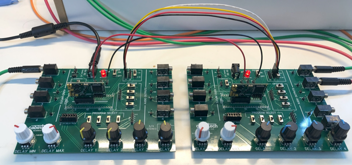
Linked development boards
(Note the photo shows V1 development boards). For secondary module boards, the jumper in the LINK section can be set to “1 CH” for single channel linking, or “2 CH” for dual channel linking.
Schematic
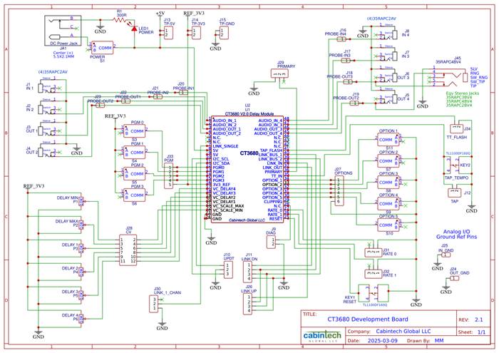
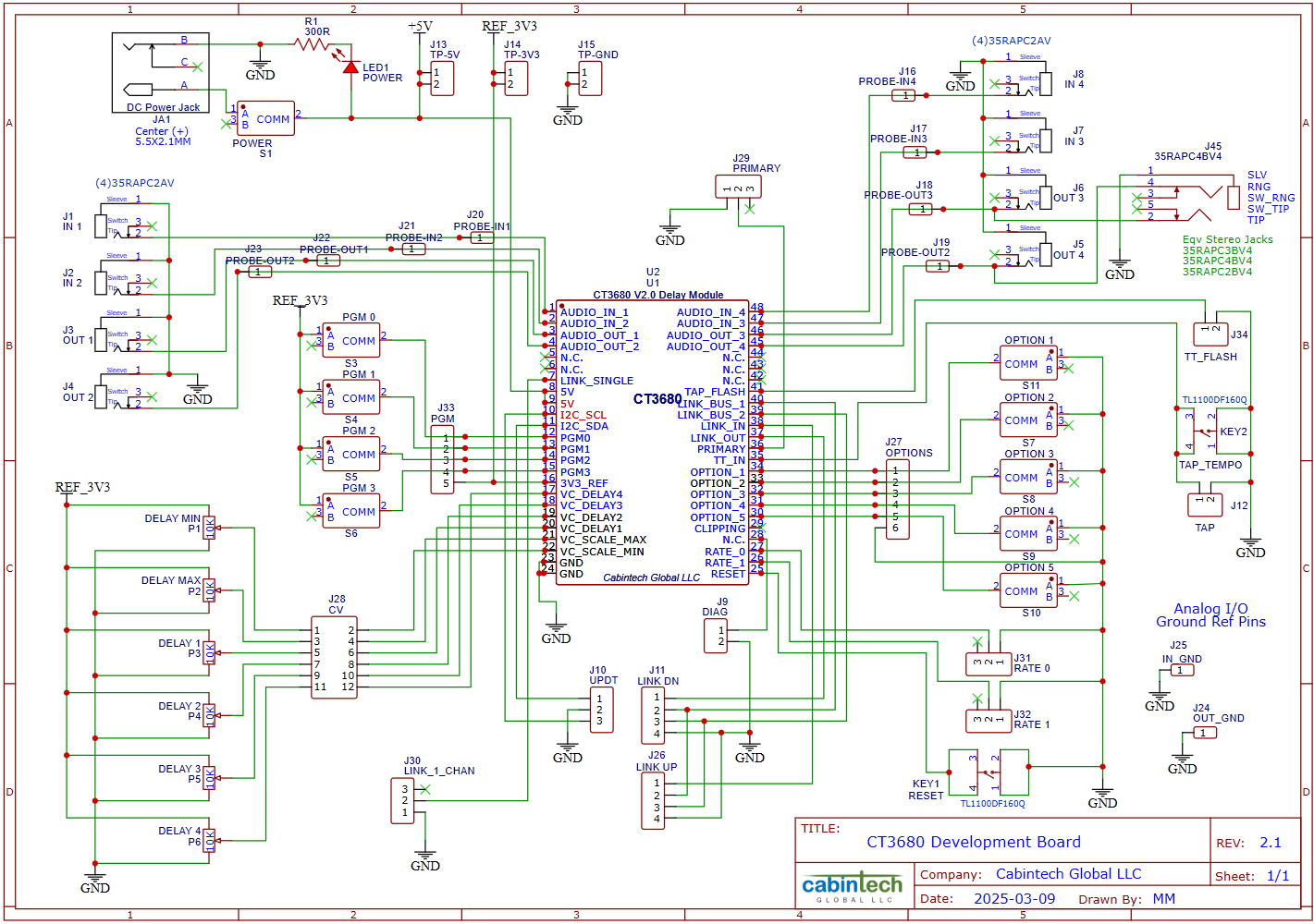
Revisions
|
Rev |
Date |
Changes |
|
Rev 1 |
April 29, 2024 |
First public release |
|
Rev 2 |
May 9, 2024 |
Added Program 6 description (General BBD Emulation) |
|
Rev 3 |
May 13, 2024 |
Updated development board details |
|
Rev 4 |
June 10, 2024 |
Revised for V1.1 of the hardware |
|
Rev 5 |
Aug 12, 2024 |
Revised for V2.0 of the hardware - Removed edge connector, added castellated edge pins - I/O pinout changed - Support for multiple sampling rates - Documented pins for firmware updating |
|
Rev 7 |
Apr, 2025 |
Updated Specifications section with measured test results |
|
Rev 8 |
Sept, 2025 |
Updated for firmware rev R3 - Tap tempo support - Removed use of the term “tap” with respect to channel outputs to avoid confusion with the new “tap tempo” support - Added Multi-Effects programs (#7 and #8) - PREVIEW FEATURE: Exponential CV delay control - Minor firmware and documentation updates |
|
Rev 9 |
July, 2026 |
Revised for V2.1C of the hardware - LED outputs (TT flasher and CLIP) can now directly drive an LED without an external current driver (8 mA max). Backward compatible with existing designs that use a current driver circuit for external LEDs. - The on-board CLIP LED is now blue instead of red. - The white LED is dedicated to tap-tempo and does not flash the program number when a new program is selected. |
Disclaimers
Features and specifications of Cabintech products are subject to change without notice. While Cabintech Global LLC strives to provide accurate and reliable information, no responsibility is assumed for use of its products, infringement of intellectual property, or other rights of third parties as a result of such use.
Cabintech Global LLC assumes no liability for applications assistance or customer product design. Customers are responsible for their products and applications using Cabintech Global LLC components. To minimize the risks associated with customer products and applications, customers should provide adequate design and operating safeguards.
SAFETY-CRITICAL, MILITARY, AND AUTOMOTIVE APPLICATIONS DISCLAIMER: Cabintech Global LLC products are not designed for and must not be used in connection with any applications where the failure of such products would reasonably be expected to result in significant personal injury or death (“Safety-Critical Applications”). Safety-Critical Applications include, without limitation, life support devices and systems, equipment or systems for the operation of nuclear facilities and weapons systems. Cabintech Global LLC products are not designed nor intended for use in military or aerospace applications or environments. Cabintech Global LLC products are not designed nor intended for use in automotive applications.
[1] The delay at an output is the ratio of the CV to 3.3V, multiplied by the delay range (max-min), plus the min. For example, output 1 delay = (0.44V / 3.3V) * (682ms – 0.3ms) + 0.3ms = 91.2ms.
[2] MinDelay + (MaxDelay-MinDelay)*(CVInput/3.3V) = 5.12ms + (51.2ms-5.12ms)*(2.8V/3.3V) = 44.2ms
[3] MaxClock - ((MaxClock-MinClock)*(CVInput/3.3V)) = 100kHz - (100kHz-10kHz)*(2.8V/3.3V) = 23.6kHz
[4] Programs 7 and 8 do not use the CV_SCALE_MAX input for scaling. Those programs set the channel max delay time to the tap interval.